Understanding Computational Lithography in One Article
Understanding Computational Lithography in One Article
Recently, Nvidia launched a computing lithography software has attracted wide attention, which makes the field has attracted more attention. The field of computational lithography has existed for 30 years, but why is it so popular now? Because it's about the continuing evolution of Moore's Law, and the continued miniaturization of chips.
01 What is computing lithography?
Before talking about computational lithography, let's start with a simple camera. We are familiar with digital cameras. Generally speaking, the larger the aperture of the camera, the better. So how to tell the size of the aperture? The number around the camera lens that looks like proportions is the size of the aperture, 1: XX, so the smaller the denominator, the larger the aperture, but the smaller the denominator, the more expensive it is.
Photography in chip manufacturing is quite similar to this principle. In the process of chip manufacturing, there is a key step in lithography, using the world's most complex "camera" at the diffraction limit, which is now known as the lithography machine. To image the microtransistors, large lenses are needed.
Rayleigh criterion (Rayleigh Criterion) —— CD=k1 * λ / NA.
Among them, the CD eigen value is the minimum accuracy that the lithography system can enlarge (that is, the resolution of the optical system), the smaller the CD value, the higher the resolution, we now call the 5nm, 3nm process is this parameter;
λ Represents the wavelength of the light source, the smaller the wavelength, the better;
NA represents the numerical aperture, representing the number of features of the lens quality. The numerical aperture is the parameter that measures the ability of the lens system to collect and focus the light. The higher the NA, the better.
Over the past 30 years, chips have been moving forward along the Moore's Law guidelines, and the microprocess has played a big role, meaning that the above CD features are getting smaller and smaller. Photography giant ASML has been using lithography machines to reduce the wavelength (λ) of the incident light source, improve the numerical aperture, and then obtain smaller and smaller CD values. ASML evolved from g-line lithography to DUV lithography and now EUV lithography. For example, in the DUV lithography machine, 249nm and 193nm are the most common wavelength (λ), and the light source wavelength of the EUV lithography system is 13.5nm.
But as can be seen in the figure below, the white straight line indicates the size of the chip. As time goes by, the size of the chip decreases exponentially, and the gold one is the wavelength of the light used for imaging. It can be seen that the gap between the wavelength and the transistor to be imaged has been widening. When this happens, physical diffraction blur the image.
Therefore, the solution given by the industry is to adopt reverse lithography thinking, first given an image, namely the circuit design on the wafer, reverse infer the required mask and light source, which is the so-called computational lithography.
According to Sisi, when sizes are very small, features are closer to each other, usually unable to clearly and accurately carve the mask pattern on the wafer. Light diffuse emission can affect the resolution, causing pattern blur or distortion. The role of computational lithography is to compensate for any image error due by diffraction or optical, resist and etching proximity effects.
Computational lithography usually includes four major technologies: optical proximity effect correction (OPC), light source-mask collaborative optimization technology (SMO), multiple graphics technology (MPT), and inversion lithography technology (ILT). Among them, OPC (optical proximity correction) and ILT (reverse lithography) are the main two types.
Computational lithography actually belongs to the category of software. ASML's definition of computational lithography is to use computer modeling, simulation, and data analysis to predict, correct, optimize, and validate the imaging performance of lithography under a series of patterns, processes, and system conditions. Computational lithography is called by ASML as the backbone of the "Iron Triangle" software section, which shows its importance.(Incidentally, ASML currently has job openings for computational lithography R & D internships)
02 The problem comes, and computational lithography is becoming increasingly difficult
But now the problem is Vivek K Singh, vice president of NVIDIA Advanced Technology Group: " When I joined lithography in 1993, if you wanted to print a cross on a wafer, you just had to print a cross on a mask. But soon that changes, and the spread of light affects the resolution, leading to blur or distortion, meaning that important elements of the chip may be missed. As shown below, some cute dog ears and hammerhead sharks began to appear on the mask as a way to compensate for the optical diffraction. But that was not enough. We had to use a fully mature optical proximity correction (OPC) -based model, and later began to enhance it with rule-based AIDS. From the simplest to the distorted mask, the end result is to print the cross on the wafer, only in a small wafer size.”
It can be seen that when the key size of the chip is smaller than the wavelength of the light source, the mask required is more and more complex. Making masks for chips in the manufacturing process has been a key step in semiconductor manufacturing for decades.
In particular, the chip gradually comes to 3nm and below, which not only requires more accurate lithography computing, but also the lithography computing takes longer and longer time. Computational lithography is a complex computation involving electromagnetic physics, photochemistry, computational geometry, iterative optimization, and distributed computation. It is difficult to achieve such a complex mask design without more powerful computational lithography.
Generdries like TSMC require a large number of data centers to process related computing and simulation operations, and their data centers usually have the CPU as the core. The figure below shows the number of CPU working hours per year estimated by Vivek Singh. The left y-axis shows that the optical proximity correction (OPC) at 2nm and 1nm requires the CPU to calculate millions of hours as the process node continues to shrink. On the right Y axis is the number of data centers used by different process nodes. The 5nm nodes need almost three large data centers, and each data center needs to process 10 masks. The 3nm nodes require six data centers, and if this continues, it probably needs 100 data centers at 1nm."You can't keep adding data centers. Something has to be abandoned. It's already snowing in Los Angeles."Said Vivek Singh. Moreover, the computing power now is likely to be insufficient in the future.
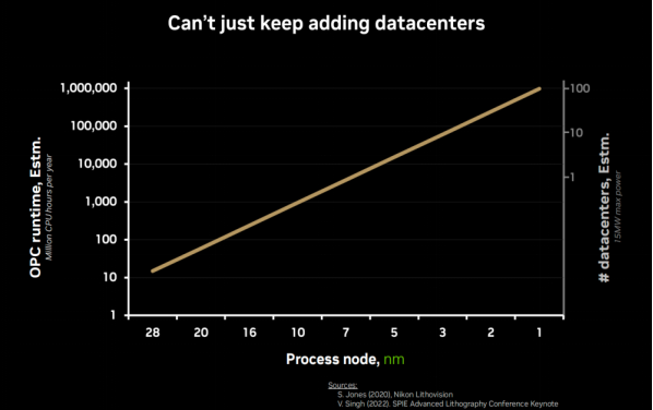
So, the computational time cost of very large workloads in semiconductor manufacturing has made Moore's Law no longer economical. The step of computational lithography has also become a bottleneck in bringing new nanotechnology nodes and computer architectures to market.
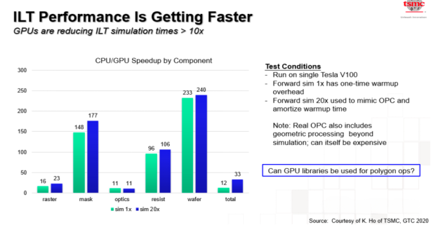
In 2020, TSMC mentioned at a meeting that using a GPU can reduce the reverse lithography (ILT) simulation time by more than 10 times. Ppt The last TSMC raises a very important question, can the GPU library be used for polygon operations?
03 Nvidia is the game-changer
Nvidia proved it today, yes. Why GPU can be used for computational lithography is because at least half of the OPC and ILT in computational lithography are composed of preimaging, and it is almost entirely composed of convolution operations, which is exactly what GPU is good at.
At the recent GTC conference, Nvidia built a cuLitho computing lithography software library on top of the GPU, the result of four years of secret development by Nvidia. Several techniques are available in the cuLitho computational lithography software library, as shown in the following figures, cuDOP for diffraction optics, cuCompGeo for computational geometry, cuOASIS for optimization, and cuHierarchy for AI.
cuLitho Has been adopted by EDA tool manufacturer Sisi, cuLitho has been integrated into Proteus full-chip mask synthesis solution and Proteus ILT reverse lithography technology. Generally, fabs need to modify OPC when changing the process, so they encounter bottlenecks.cuLitho Can not only help break through these bottlenecks, but also provide new solutions and innovative technologies needed by new technologies such as curved photomask, High-NA EUV lithography, and subatomic photoresist modeling.
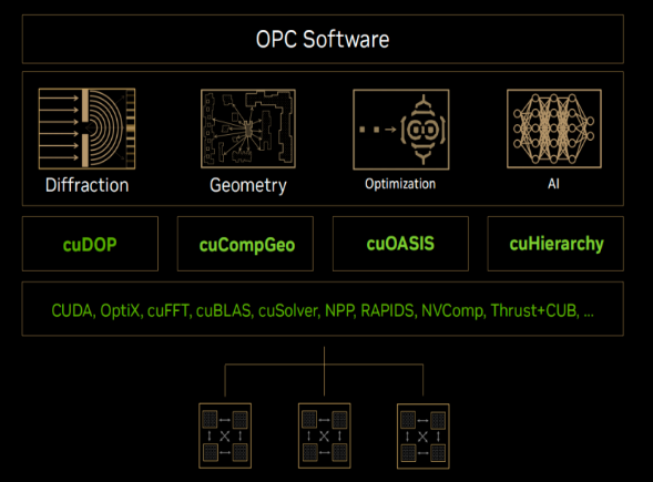
cuLitho Is the core of a set of parallel algorithm, invented by nvidia scientists, calculate all parts of the lithography process can run in parallel, originally need 40000 CPU system to complete the work, now only 500 NVIDIA DGX H100 system can be completed, this not only greatly accelerate the current annual consumption tens of billions of CPU hours of large-scale computing workload, and reduce the power consumption and the impact on the environment.
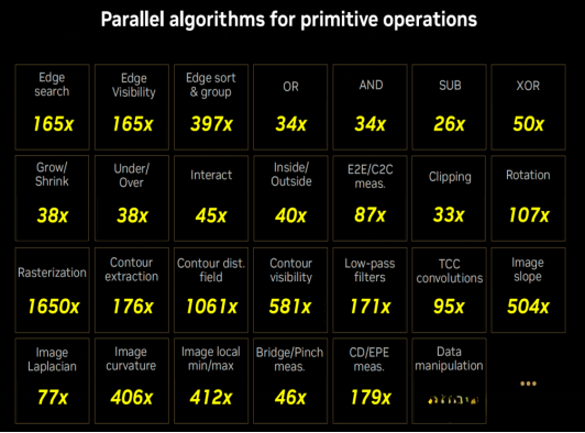
cuLitho One continuous CPU operations at the component level, with a 138 x improvement on the Ampere component and a 254 x increase on the Hopper structure. In the end-to-end OPC project, combined Ampere increased 23 times and 42 times on Hopper.
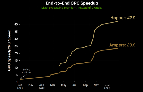
Wafs using cuLitho can increase photomask production by 3-5 times per day, while power consumption can be 9 times lower than in the current configuration. Nvidia says the cuLitho computing lithography based on the GPU is 40 times better than the current lithography process, and a photomask that would have taken two weeks can now be done overnight.For example, the Nvidia H100 GPU requires 89 mask plates, taking two weeks to process a single mask plate when running on a CPU, and only 8 hours to run an cuLitho on a GPU.
In the long run, cuLitho will bring better design rules, higher density and production, and AI-driven photolithography, allowing the fabs to increase production, reduce their carbon footprint and lay the foundation for 2 nm and higher processes.
cuLitho Computational lithography software library, has been TSMC and ASML cooperation.cuLitho will be in use at TSMC in June, TSMC to deploy inversion lithography, deep learning, etc.; ASML plans to add GPU support to all computational lithography software products, cuLitho advantages will become particularly obvious in the High-NA EUV lithography era; EDA tool vendor Synopsys OPC software will run on the cuLitho platform.
Below is an chromeless face shift mask. If you put it into the ASML's latest lithography machine, what pattern will come out?
The answer is, the NVIDIA cuLitho.
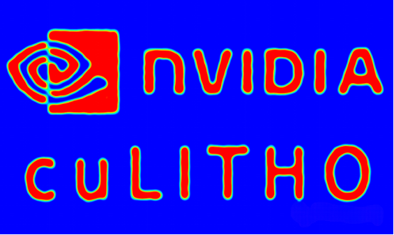
The current cuLitho computational lithography is just a mathematical tool for Maxwell's equations, but Nvidia says AI-based computational lithography is "under development". Imagine what had happened if AI technology had introduced computational lithography?
04 is written at the end
Without the support of computational lithography, chipmakers would be able to create the latest technology nodes.cuLitho The release of computational lithography library software not only provides an innovative technology for the continued evolution of chips, but also once again plays the potential of GPU —— from the initial graphics processing to AI chips, to the data center, and even the future of chips.
To borrow the hardware and software fusion books and the public author, Shanghai moment to the founder and CEO of science and technology Huang Chaobo on the release review: " old huang is very successful, but actually essentially old huang only do one thing (parallel computing) and two aspects (GPU is parallel computing platform, CUDA is in order to better parallel computing programming).”
Every time a chip reaches a bottleneck, new technologies, such as the FinFET transistor invention, have survived Moore's Law for more than a decade. Now, in order to keep the chip miniature, various new materials, new architectures, new packaging, new interconnection and other technologies are emerging.