What is EDA and the application and prediction of EDA
What is EDA and the application and prediction of EDA
1. Preface
In recent years, artificial intelligence (AI) and machine learning (ML) have made breakthroughs in many application fields. In the traditional semiconductor field, researchers have also explored new methods of chip design based on machine learning. These new algorithms are often first reflected in the chip design tools, also known as the EDA tools. Therefore, this research direction can often be called ML for hardware design, or ML for EDA (strictly more extensive). Sometimes also called do intelligent EDA algorithm or intelligent IC design method. This paper will introduce the hot research direction of ML for EDA in the field of EDA. This direction involves machine learning, data structure and algorithm, circuit design and manufacturing and other basic knowledge, which is a typical crossover research direction. We will start with the background knowledge of EDA and introduce what ML for EDA is, why we study ML for EDA, some early representative work in the research direction, the current process of commercialization, other relevant research directions, and the challenges ML for EDA may face.
2. What is an EDA? EDA and the chip design foundation
Chips are everywhere in our lives. The design and implementation of the chip involves a complex process. Taking the digital chip as an example, if the design team starts from the completed Verilog / VHDL code, the standard design process should include at least logical synthesis (logic synthesis), layout planning (floorplan), clock tree synthesis (CTS), layout wiring (placement & routing) and other steps. In addition, we also need to do a lot of simulation and verification work. In this process, engineers need to weigh multiple design goals, such as power consumption, frequency, and area, while also making sure that the manufactured chip will function correctly. Moreover, with Moore's Law, large-scale chips can contain more than 10 billion transistors. Given the complexity of this process and design, almost all design teams need commercial EDA tools to assist in completing the entire chip design. So if we compare the entire semiconductor industry to a gold mine, the EDA tool could perhaps be seen as a mining shovel. At a time when the United States frequently restricts semiconductor exports, the EDA industry, which has a small market value, is paying more and more attention. The full name of EDA is Electronic Design Automation, or electronic design automation. After decades of development, EDA tools have been used in every aspect of the chip design and manufacturing process. The quality of the EDA tool will affect the quality of the final chip (power consumption, frequency, area) and design efficiency (time to market). Therefore, the goals of EDA algorithm researchers usually include at least two aspects, one is the chip optimization effect (power consumption, frequency, area), and the efficiency of the EDA tool itself (total time spent = single run time of the tool * the number of times to use the tool). Here we highlight the number of times the EDA tool is used because the chip design is not done at once. Usually engineers need to iterate the design steps several times until the design goal are achieved. At each iteration, engineers can modify the tool parameters or the chip design, and rerun the EDA tool for better chip results. For large-scale chip design, only part of the design process can take days to weeks each time. Therefore, the more iterations, the more time is spent on the EDA tool, and the later the final stream and product launch date will be. As we will see later, the principle of many ML for EDA work is to reduce the number of iterations and bring the chip quality back to the design goal as soon as possible.
3. What is a ML for EDA? Prediction and optimization
In recent years, we have seen more and more exploration in the ML for EDA directions. As shown in Figure [1] below, presented in representative EDA meetings (DAC, ICCAD, ASP-DAC,...) The number of work related to journals (TCAD) has increased year by year.
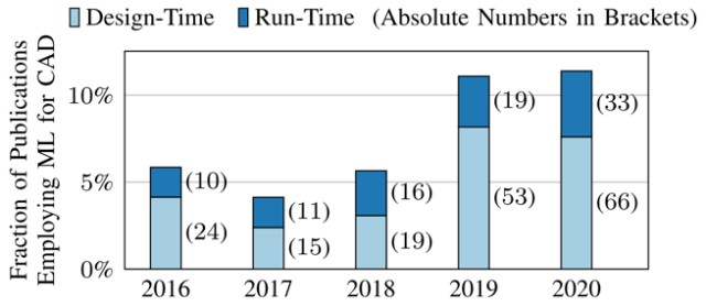
Figure 1 The number of ML for EDA papers published over the years The role of these ML for EDA methods in the chip design process can be roughly divided into prediction (prediction) and optimization (optimization). We will present these two types of applications as examples, respectively. Predictive class work usually uses ML models to make early rapid prediction of the final goal of chip optimization. Using the prediction of the ML model, designers can reduce the use of time-consuming EDA tools while directly predicting the approximate effect of the EDA tool after running. Based on the ML prediction, the designers can adjust the design parameters in time. In other words, the ML model reduces the number of runs of the EDA tool by rapidly predicting the behavior of the EDA tool. A typical example of prediction work is using the CNN model to predict [2] of DRC hotspots (hotspot) before the chip winding. DRC hotspots refer to the areas that violate the design rules after winding. By forecasting, the EDA tool can try to modify the layout in advance to avoid DRC hotspots that will occur in future stages. This work can be compared to image classification or semantic segmentation with CNN, where the chip layout is similar to the picture, and the predicted DRC hotspot position is similar to the block required to be segmented on the image.
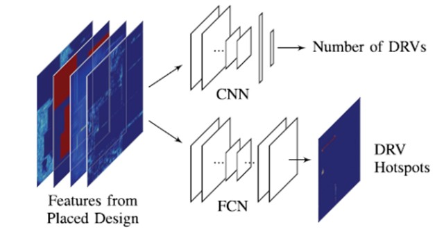
Figure 2 Prediction class method for example: Using CNN to predict DRC hotspots [2] Compared with prediction class work, optimization class work needs to be done more. The optimization here is a broad concept, referring to directly solve some of the EDA problems. In fact, a large number of EDA problems are essentially chip optimization problems under certain constraints, and many traditional EDA algorithms are excellent heuristic solutions (for these problems) accumulated over the years. Then the optimization class ML method pursues a better or faster solution than the traditional EDA algorithm. This solution can help to generate realistic and accurate chip design results. A typical example of optimization is Google using reinforcement learning (Reinforcement Learning) for macro placement (placement) [3]. Through the reinforcement learning algorithm, this work can be compared to AlphaGo, where the chip layout is similar to the Go board, and the position of each macro element is similar to the best position of each game.

Figure 3 Using reinforcement learning Following this less strict classification, the prediction ML method can reduce the use of EDA algorithm, thus improving the efficiency of chip design. Optimizing the class ML method can help to generate faster or better designs. If we want to completely replace some traditional EDA algorithms, we need the optimization class method. Of course, it is difficult to directly replace the traditional EDA methods for large-scale optimization problems including million elements. At present, we see that more ML methods are integrated into the EDA framework, which plays an important auxiliary role in .
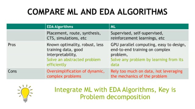
Figure 4 Comparison of the EDA and ML methods: ML should be integrated into the EDA method
4. Why study ML for EDA?
Before reaching out to other work, one question that needs to be answered is, why are we study ML for EDA? In other words, what are the core advantages of ML for EDA over traditional EDA algorithms? Here is an attempt to provide a simplistic explanation of the . As introduced in the background, the design process is divided into multiple stages. In most stages, it is difficult for EDA tools to directly optimize the final design goal, because the final design goal is only determined after the entire process is completed. Thus, the EDA tool can only make a rough estimate of the final design goal. For example, the layout (placement) algorithm may optimize bus length (HPWL) and congestion (congestion), but this optimization goal does not always reflect the final design goal (final chip power consumption, frequency, area, DRC hotspot, etc.). Therefore, unless you go through a long design process, the early EDA tool is not good enough each time. To ensure convergence of the design, one strategy is to use conservative early estimates to leave sufficient room for later stages (margin). But that will obviously sacrifice the chip quality. Another strategy is to constantly adjust the parameters for repeated iterations in order to obtain better chip quality. This relies heavily on the experience of professional designers and takes a lot of design time. The ML for EDA algorithm is characterized as it is a data-driven method. By learning existing design data, early use of ML prediction can achieve a more accurate final optimization goal as an important early feedback (early feedback). Therefore, the prediction-class ML approach breaks through the obstacles before different design stages. As for optimization-class ML methods, reinforcement learning type methods are possible to obtain better solutions than traditional heuristic algorithms by exploring huge design space. In addition, some ML methods can learn from the optimization experience of engineers, reducing the reliance on the engineer experience. Finally, ML methods are usually very fast when prediction, so ML methods will have orders of magnitude advantage over traditional methods.
5. Representative ML for EDA study work
In fact, ML for EDA's work goes far beyond the two previous examples. And these work can be classified in multiple ways. If we classify ML according to the stage or step of ML application, ML has been tried by researchers for the vast majority of design stages. According to the summary of relevant articles [1], the application of ML model stage can include 1. High order synthesis (HLS) and design space search (DSE), 2. logical synthesis, 3. Physical design (from layout planning to wiring), 4. photolithography and manufacturing, 5. Verification and testing. In addition to opening digital circuits, some ML studies also have some attempts at the layout and wiring of analog circuits.
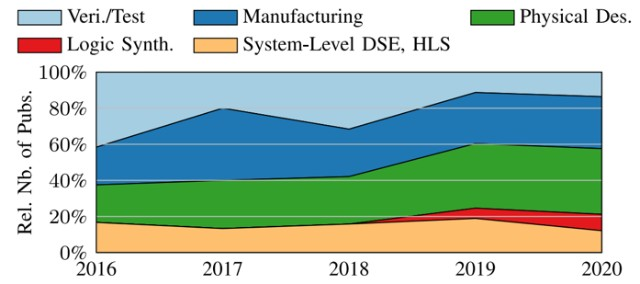
Figure 5 Proportion of ML for EDA papers applied in different design stages in calendar years If we classify according to the ML prediction or optimized target, ML has been tried by researchers for most of the chip optimization targets, Including, but not limited to:
1. Power consumption (power),
2. Frequency and delay (delay or slack),
3. Area and line length,
4. Congestion (congestion) and rule checking (DRC),
5. Voltage drop (IR drop) and crosstalk (crosstalk),
6. Manufacturability (Manufacturability).
The following is a brief list of some specific ML for EDA work. Space limit, obviously difficult to exhaust. Therefore, try to list earlier and higher cited work in the same type. For an updated and more complete summary of ML for EDA work, the reader can refer to paper , or Video . For the FPGA platform, in the high-order synthesis (HLS) stage, there are work trained ML models to predict the utilization of the final FPGA resource and whether the timing converges . The predicted FPGA resources include RAM, FF, LUT and DSP, etc. The ML model is either the MLP or the XGBoost.
The input, output, and use phase of the ML model are shown in the figure below.
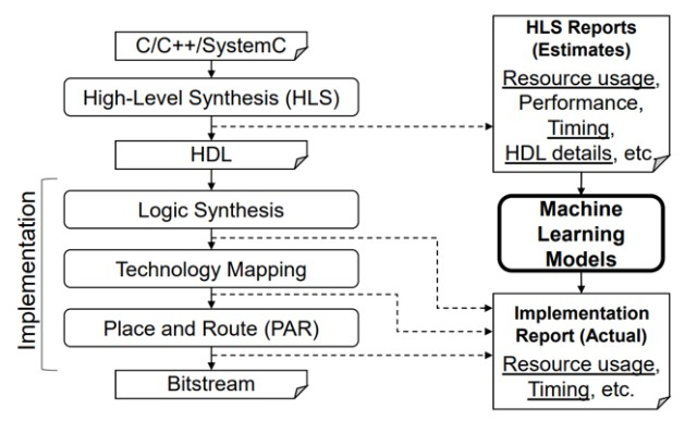
Figure 6 Preof FPGA resource utilization in HLS stage .Also in HLS stage, ML can conduct design space exploration (DSE) The basic method is to guide each sampling with the prediction results of the ML model, and then retrain the ML model according to the sampling results, and repeatedly cycle until the design of sampling obtains good enough results. The ML model used here is a random forest (RF). Such exploration tasks are also not limited to higher-order synthesis. For example, the popular problem of adjusting the parameter of EDA tools with ML also belongs to a similar spatial search task.
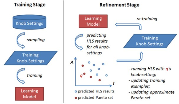
Figure 7 Design space exploration (DSE) with ML (Random forest) In the RTL stage, ML can be used to quickly estimate for the power consumption after logical synthesis. In other words, the ML model simulates the fast power consumption early in the design. The input of the ML model is the flip value of all RTL signals in each cycle of the chip (1 represents the signal flip, 0 represents the constant signal in that cycle), while the output is the total power consumption of each cycle of the chip. This input was chosen because the dynamic power consumption of the chip is positively correlated with the flipping rate of the logic gate. This work tries various basic ML models including linear regression, PCA dimension reduction, and CNN.
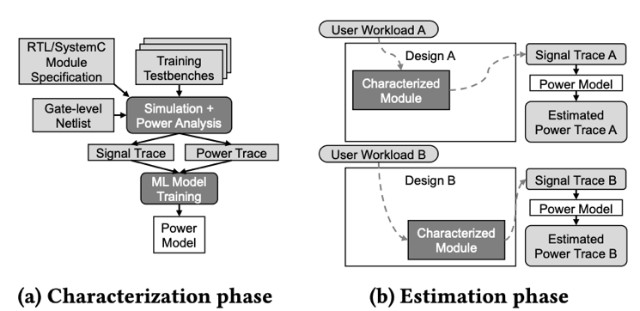
Figure 8 uses ML model (CNN or linear model) to simulate the chip power consumption of each cycle In the stage of logic synthesis, ML model can be used to select [9] for the process of logic synthesis. Here the ML model is trained to predict the combination of synthesis transformation that best fits the current chip design. This work encodes various combinations of transformation into two-dimensional matrices, and then deals with CNN models to predict whether they are good or bad processes.
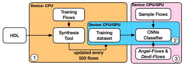
Figure 9 Select the appropriate logical synthesis process with ML (CNN model) . In the physical design (from layout planning to wiring) stage, the two examples of macro placement and DRC hotspot prediction mentioned at the beginning both belong to this stage. Another example is the prediction of the for the voltage drop (IR drop) distribution on the chip. Similar to the previous example, the CNN model can predict hot spots with too high IR drop (hotspot). Here, the input to the model is the instantaneous power consumption distribution. The predicted IR drop is positively correlated with the instantaneous power consumption within the region.
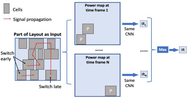
Figure 10 Predicting the voltage drop (IR drop) hotspot with ML (CNN model) . In addition to the above work for digital circuits, there is also a lot of exploration of analog circuits. One example is the direct guidance (guidance) of the analog circuit winding . The ML model used here is a Variational autoencoder (VAE). The input to this VAE model comes from the analog circuit layout before the winding.
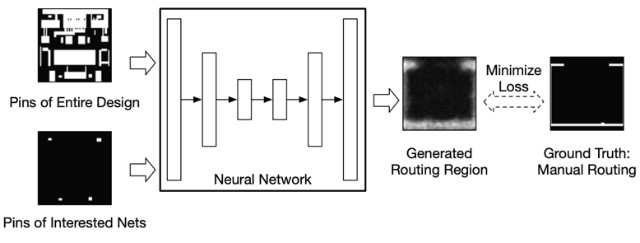
Figure 11 After using the ML (VAE model) auxiliary analog circuit winding design, a mask (mask) for the lithography machine is generated for chip fabrication. For the advanced process, optical proximity correction (OPC) is an important step in the process of mask generation in order to get and design the same figure on the wafer. The ML can be used to perform the OPC . This work uses a generative adversarial network (GAN) to quickly generate masks after the OPC.

Figure 12 Optical proximity correction (OPC) process using ML (GAN model) In addition to improve manufacturing yield (yield), lithography (lithography) hotspot (hotspot detection) is required. Photolthography hotspots are areas where short circuits or open breaks may occur after manufacture. ML can be used to predict the lithography hotspot . This work performs a discrete cosine transformation (DCT), and then uses a CNN model to determine whether the region is a lithography hotspot.

Figure 13 detects for lithography (lithography) hotspots using ML (CNN model)
6. Representative ML for EDA business exploration
In addition to academic exploration, EDA companies and chip design companies have also shown great interest in the direction of ML for EDA. Two major EDA companies, Cadence and Synopsys, have launched commercial products that incorporate some ML algorithms. For example, Cadence's physical design tool, Innovus, already integrates some machine learning tools in the new version, such as providing a more accurate estimation of the (post-wiring) timing before the wiring (routing). This ML feature seems to get some good reviews for . In addition, the sign-off tool Project Virtus (Voltus + Tempus) also used ML . More influential is Cadence's Cerebus tool, which adjusts the design process of RTL-to-GDS II through the ML model based on reinforcement learning, and reduces the reliance of on artificial designers. But as relevant practitioners, it is difficult to understand the technical details of this product, such as how the reinforcement learning algorithm here was migrated to different chip designs. Similarly, Synopsys also launched the DSO earlier. The AI tool is also used to optimize the design process automatically . The PrimeTime ECO tool for Synopsys also uses the ML model. In addition, the former Mentor Graphics (now Siemens) has also introduced an optical proximity effect correction (OPC) tool based on ML prediction. In addition to EDA, the research team at Google and Nvidia is also actively exploring ML for EDA directions. These are the more research-oriented work. For details, refer to Google Jeff Dean and Nvidia Bill Dally. In China, influenced by the influence of American semiconductor policy, many excellent domestic EDA startups have emerged in recent years. Some companies have also begun to explore the application of ML in the EDA field. For example, a domestic company recently released a tool based on machine learning technology and layout planning, which should be similar to the Google macro placement algorithm mentioned above. Personally, I think this is a more challenging task.
7 Other studies related to ML for EDA
In addition to the work introduced above, there are also some hot research directions that are often classified into ML for EDA research. But strictly speaking, I personally think that these directions may not completely belong to the narrow sense of the ML for EDA category. Using GPU to accelerate the EDA algorithm is a very hot research direction in recent years. For example, use the GPU to accelerate the layout process . These methods cleverly take advantage of the similarity of the optimization process of the EDA problem to the deep learning training process. So they can use existing deep learning frameworks, such as PyTorch, for rapid GPU-based optimization. However, such methods will not apply specific ML models, and there is no data-based training process.
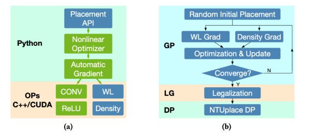
Figure 14 Using a GPU to accelerate the chip layout process [18] Another direction often classified as a ML for EDA is to implement the ML model on the chip for monitoring, control, or management when the chip runs. For example, using the ML method, develop an on-chip real-time power consumption detection tool [19]. The purpose of using ML methods is to reduce the hardware overhead of this model on the chip. Strictly speaking, this is closer to chip design than to EDA tools, perhaps classifying it into ML for hardware design categories.
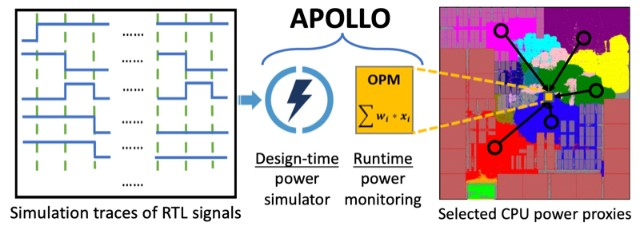
Figure 15 uses the high-efficiency on-chip power consumption detection model developed by ML.
8 ML for EDA
Finally, a brief summary of some of the challenges ML for EDA may face. In recent years, some attempts have been made in recent years. First, the chip design data required for training are very difficult to obtain. For this problem, on the one hand, some researchers began to provide the publicly available chip design dataset . On the other hand, the researchers explored the model training under the protected data privacy conditions, such as the federated learning-based method , or some encryption of the training data. Second, developing and maintaining ML models requires a large number of engineers with ML background, which is not easy for semiconductor companies. In order to further enhance the degree of automation, the researchers explored some automated ML model development methods. These works are generally based on the existing AutoML or neural network architecture search (NAS) methods in the field of deep learning, and then some customized design for specific problems. Third, mobility of ML method accuracy is difficult to guarantee due to differences between chip design and process. In addition, the safety and reliability of ML method also needs more guarantee. There have been many preliminary studies on the safety and reliability of ML methods. Some summaries are provided in the paper. Fourth, from a practical engineering perspective, how to better integrate the ML method into the existing EDA tools and chip design process. This may need to be explored together by the researchers and the industry.