Nanoimprinting, finally coming to the stage?
Nanoimprinting, finally coming to the stage?
Today, ASML is almost synonymous with lithography machines. Especially with the launch of EUV and even High-NA EUV lithography machines, ASML is dominating the high-end lithography machine market.
As we all know, lithography is the most important, complex and expensive process step in the chip manufacturing process, accounting for more than 30% of the total production cost, and accounting for nearly 50% of the production cycle.
For decades, Moore's Law has been continued with the support of DUV and EUV lithography machines. However, since the iteration, in the face of the chip transistor line width approaching the physical limit, and the limited capacity and high cost of EUV lithography, the industry has begun to explore the technology and process of bypassing EUV lithography to produce high-end chips.
Among them, nano imprint technology (NIL) came to the forefront.
Recently, it was revealed that SK Hynix introduced a nano imprint device from Canon, which is currently undergoing testing. It plans to start mass production of 3D NAND flash memory around 2025, and the test results so far are good.
The nanoimprint technology mentioned here is the next generation of lithography that is considered the most likely to replace EUV.
01 How to mark EUV lithography?
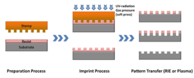
Nano-imprint technology, namely Nanoimprint Lithography (NIL), is a new type of micro-nano processing technology. The technique designs and makes tiny figures on a template to a silicon substrate coated with polymer materials by technology such as emboprinting. The resolution of the nano imprint is determined by the size of the print template pattern used. There is no diffraction limit in the lithography physically, and the nano imprint technology can realize the nano-scale line width pattern.
Can be understood as, nano imprint technology make chip like stamp, the gate length is only a few nanometers circuit engraved on the seal (mask), and the seal on the putty (imprint), realize graphics transfer, and then through the heat or UV light transfer the method of graph curing, to complete the micro and nano processing "carving" steps.
Nanoscale printing is replaced by lithography link, only the lithography step is replaced by nanorepression technology, other etching, ion injection, film deposition of these standard chip manufacturing processes are fully compatible, can be very good access to the existing industry, without overturning.
The essence of lithography is that the mask plate is patterned for the photoresist to achieve patterned deposition and etching processes. The final resolution of the lithography process is determined by the wavelength of the light source used.
Optical lithography, which the industry now relies on, has many limitations:
SDAP and SAQP processes are two-dimensional pattern solutions, which severely restrict the design layout;
Due to the limited accuracy, to expose more sophisticated chip lines, but also need to use multiple exposure technology;
Improving optical lithography resolution is mainly achieved by shortening the wavelength of lithography light source, although the light source has been shortened from ultraviolet 436nm, 365nm to deep UV (DUV) 193nm and extreme ultraviolet (EUV) 13.5 nm, but in the optical diffraction limit, the resolution limit is about half a wavelength;
The shortened wavelength of lithography light source makes the difficulty and cost of lithography equipment doubled, and its cost and scale ability have been unable to match the trend established in the past 25 years.
Therefore, the industry began to hope for nano-imprint lithography technology.
Any new lithography technology introduced in chip fabrication must provide either a performance advantage or a cost advantage.
Compared with the traditional lithography technology, first of all, the nano-imprint printing technology does not require a complex optical path system and expensive light sources, which can greatly reduce the manufacturing cost.
In addition, the nanosized imprint template is simpler than the mask pattern design used in the lithography machine, and the size of the printed pattern is completely determined by the pattern on the template, so it will not be limited and affected by the light source wavelength and optical diffraction in the traditional photoresist technology. Nano-imprint technology faithfully reproduces patterns with higher resolution and greater uniformity compared to the patterns produced by lithography devices.
At the same time, as long as the nano-imprinting technology is made on the mask in advance, even the complex structure can be formed at one time, and at the same time, it avoids the repeated exposure in the traditional lithography process, which further improves the cost advantage. Nanoimprinting can save part of the costly lithography process, which can reduce the manufacturing cost of the process by 40 percent and power consumption by 90 percent compared to The Nikkei.
In addition, nano imprint technology has its unique advantages in three-dimensional structure processing. Traditional lithography technology is based on two-dimensional plane processing, it is difficult to obtain three-dimensional structure, and the controllability is poor, but for nano imprint technology, as long as the template, can be mass production of three-dimensional products.
02 Nanometer imprint technology, breakthrough and challenge coexist
In 1995, Chinese scientist Professor Zhou Yu (Stephen Chou) proposed the concept of nano imprint printing for the first time, which opened the prelude to the research of nano imprint manufacturing technology.
By 2003, nano-imprint, as a micro-nano processing technology, was included in the International Semiconductor Technology Blueprint (ITRS).
In 2009, Molecular Imprints (MII), which is engaged in the development of nano printing technology, planned to use NIL technology for the production of 32nm logic nodes. But —— is said to be due to slow production speed and high defect rate, and funding problems as a constraint on MII technology development.
Five years later, in 2014, Canon acquired MII. In fact, a decade ago, Canon began secretly developing nano-imprinting technology in 2004, until it acquired MII company and renamed it Canon Nanotechnologies to enter the NIL market.
Since then, Canon and Toshiba have jointly developed NIL technology —— Toshiba (Toshiba memory was renamed Kai Xia in 2019) has long wanted to use NIL in flat NAND flash memory manufacturing. However, it seems that 193nm lithography and multiple exposure can reduce the NAND cell size from 120nm to 1 xnm node; at this node, the storage cell and floating grid.
As a result, NAND began to evolve to 3D, and Toshiba also turned to the application of NIL technology. About five or six years ago, Toshiba said the lithography demand for non-volatile memory devices is moving from higher resolution to lower cost, so it plans to use NIL in the 3D NAND era.
Since then, there has been news that Canon has used nanoimprint technology for mass production of memory chips.
It is understood that Canon's latest nano imprint equipment parameters have good indicators, set engraving accuracy of 2.4nm/3.2nm, can expose more than 100 wafers per hour, nano imprint technology has reached 3D NAND mass production level and requirements.
As mentioned above, in addition to Kai Xia, SK Hynix has also purchased nano imprint equipment from Canon and is testing the 3D NAND flash memory production project, which is considered the next generation of EUV lithography machines used in the industry's most cutting-edge manufacturing process.
An industry insider said: " Compared with EUV, nanoimprint technology has less freedom to form patterns, so it is expected to be a priority for the production of NAND flash memory that maintains a certain pattern."SK Hynix began to purchase equipment for this reason."If the nanoimprint equipment is commercially available, the NAND flash memory enterprises led by SK Hynix will be able to improve the production efficiency of the 3D NAND flash memory field with more difficult processes starting from the 200 layer.
On the other hand, memory chip giant Samsung Electronics also quickly introduced EUV lithography machines to solve the rising costs caused by the introduction of multi-pattern technology, in addition to developing 3-4 solutions including nano-imprinting technology.
In addition to its exploration of NAND flash memory, Canon is trying to apply NIL technology to logic chips such as DRAM and CPU.
For DRAM, Canon has been constantly improving the set engraving accuracy. The use of POI control technology, wafer area chuck control, fine mask and other methods can help to improve the accuracy of sleeve engraving.
The combination of advanced NIL tools and masks can provide a variety of solutions for many different applications, and Canon demonstrated 2.3nm set engraving accuracy for a variety of new technologies, mainly for DRAM.
In the field of chips, nano imprint lithography is better at manufacturing memory chips such as 3D NAND, DRAM and so on. Compared with logic circuits such as microprocessors, storage manufacturers have strict cost limits and relaxed defect requirements, and nano imprint lithography technology is more consistent with it.
According to Canon's future roadmap for nanoimprint equipment, the application will start with 3D NAND memory chips, gradually over DRAM, and eventually realize the manufacturing of logic chips such as CPU.
It is understood that Canon's current mass-produced nano imprinting equipment, which can be used to produce 15 nanometer chips, is expected to be in 2025, can further develop equipment to produce 5 nanometer chips. In the initial stage, it will take the lead in introducing the production of NAND, DRAM, etc. In the future, it is expected to import the logic IC production requiring advanced advanced manufacturing process for applications in PC and mobile phones.
To achieve this goal, Canon recently proposed at the French conference that it would spend more than 50 billion yen in Japan to expand its microfilm equipment capacity, and Canon said the plant will be built in 2023 and is expected to start operating in 2025. In addition to producing its existing lithography machine series, the plant will also produce nano-imprint lithography equipment.
Previously, Canon and Kai Xia, DNP (Big Japan printing) in the nano-printing technology has been a lot of cooperation. DNP 2015 Is said to have established a commercial production system for nano-imprint Templates (template); Toshiba announced plans in 2016 to build NAND flash memory.
It can be seen that Japanese companies want to catch up with ASML through semiconductor "nano imprint technology", from equipment trial production, fabs trial operation to the production of the new plant production line.
In addition, other equipment suppliers in this technology direction currently include Nanonex, EVG, SUSS MicroTec, Obducat and other European and American companies.
EVG has announced a partnership with Toppan Photomask, a photomask subsidiary, to develop NIL technology to further accelerate its application in optical micro-nano manufacturing. The first collaboration between nanostamping process equipment providers and nanoimprint plate manufacturers is a huge achievement of the industry and will help the industry rapidly expand nanoimprint as a mass-production technology and components for advanced optical equipment.
From 1995 to now, after continuous improvement and technological breakthroughs, nano-imprinting technology has been applied to LED, screen display, DNA sequencing, AR / VR, sensing and other fields.
However, its application in integrated circuit manufacturing is still in the early stage of industrialization. Currently, nanoimprint is listed as one of the representatives of next generation 32nm, 22nm and 16nm node lithography in ITRS. After nearly 30 years of research, nano-imprinting technology has made new progress in many aspects, and domestic and foreign semiconductor equipment manufacturers, material manufacturers and process manufacturers have begun to get involved in this field.
03 In the field of chip manufacturing, nanoimprint technology challenges are still there
Although the advantages of nano imprint technology are mentioned above, and is even regarded as the new hope of the industry, nano imprint technology is still some shortcomings from large-scale commercial mass production.
Good product control: nano imprint is in direct contact between the wafer and the mask, it is easy to appear defective products mixed with fine garbage and dust on the circuit. In order to achieve practical application, it is necessary to improve the manufacturing technology and application.
Template has low life and high replacement cost: whether it is DUV lithography, EUV lithography or nano imprint, the most expensive consumables are mask or imprint template. Nanoimprint template, because it is necessary to directly contact the imprint glue work, in the process of contact, there will inevitably be a variety of damage or pollution, shorten the life of the template.
Complex alignment: the embossing template needs to be accurately aligned and attached with the base table bearing the imprint glue, and the precise mechanical device is required to cooperate with the testing equipment to carry out the embossing process. However, the existing nano-stamping equipment lacks a high precision calibration mechanism in terms of parallel and vertical alignment. Although we can use the optical alignment on ultraviolet lithography, or Moore stripe technology, nano imprint not only has curing, but also the vertical imprint movement process, so it will bring multi-direction deviation.
This several problems, but not all is nano imprint technology, reduce process cost, improve the yield and improve production efficiency for the early development of the lithography machine is also to face the problem, any technology from laboratory to mature, will face these problems, all need to solve these problems in the process of development.
04 Can NIL replace EUV lithography?
Review chip lithography industry, the first 20 years of the 21st century, due to the global chip industry chain in immersion DUV, EUV projection lithography technology continued huge investment, projection lithography become the mainstream of IC manufacturing technology, born the Dutch ASML lithography equipment giant, and application level of TSMC, samsung international chip processing enterprises, nano imprint lithography gradually exit the IC manufacturing technology competition, into the silence.
With the development of the industry, DUV, EUV lithography machine and other system complexity, technical bottlenecks and cost problems are increasingly prominent, nano-stamping technology seems to usher in a new vision.
According to the maturity curve of new technology proposed by Gartner, combining the data of patents, papers and market intelligence in the course of technology development, the industrialization curve of nano stamping technology is drawn in the terms of annual and expected value dimensions.
Trigger period of the birth of science and technology: Since nano-stamping technology was proposed in 1995, it has attracted wide attention and followed up from academia and industry. At present, most of the technology and equipment providers have entered this stage.
Expected expansion period: In 2003, nano imprint technology was included into the International Semiconductor Blueprint (ITRS) for the first time, and the research and expectation of technology entered a climax. During this period, nano stamping related equipment was widely purchased by scientific research institutions.
Bubble change trough period: subject to the process is not mature, the industrialization is not as expected. A number of businesses closed or were acquired, marking Canon's acquisition of MII in 2014. However, during this period, nano imprint large area, continuous production technology has been developed to be industrialized in the production of photonic crystal LED chips.
Steady climb in the bright period: technology gradually breakthrough, in LED, microfluidic, MEMS, AR and other fields to achieve industrial application. Domestic enterprises also increase the research and development and application layout of nano-imprinting technology.
Industrialization maturity period: After 2021, with the maturity of the process and the breakthrough development of downstream application fields, nano-stamping technology may usher in a large area of industrialization.
TechNavio Data show that the nano-imprint market is expected to reach $3.3 billion in 2026, with a compound annual growth rate of 17.74% from 2021 to 2026. Nano-printing market is not as big as expected, but the overall is gradually strengthening.
Nano stamping technology has its unique advantages, but also has corresponding disadvantages. In the future scientific research and production, it is necessary to further optimize the process conditions to help expand and improve the application of nano stamping technology.
Finally, back to the core of this —— in the content of the chip manufacturing field, although Japan has completed the first practice, but can it replace EUV lithography?
To be honest, the difficulty is very big, unless TSMC, Samsung, Intel, SK Hynix and other industry manufacturers give up mature technology to nano stamping technology. In fact, we can also see from the industry dynamics, every few years there will be the news that nano imprint lithography is about to break through, but each time to delay the time into the industry.
All the signals indicate that the technology is not easy. But in the future, when optical lithography really reaches the limit and it is difficult to move forward, nano imprint technology may be a route to look forward to, and then, chip manufacturing may also usher in a new paradigm, everything will be overturned.
After all, no technology can exist for long, and if it does, just because people haven't had time to find something new to replace it.


 English


