Power semiconductors, the outcome is undecided!
Power semiconductors, the outcome is undecided!
In the past few years, wide bandgap semiconductor materials such as GaN and SiC have developed rapidly, and they have been commercialized and developed well. Therefore, everyone is full of hope that the third-generation semiconductor will rule the power semiconductor market. And expressed concern about the future of silicon power devices.
However, with the efforts of different manufacturers and institutions, this market seems to have different fixed numbers.
Silicon, not yet dead
First of all, it is necessary for us to go back to the development history of power semiconductors: as early as the late 1950s, the bipolar junction transistor (BJT) was first invented, power diodes and thyristors appeared in the 1960s, and again in the 1970s and 1980s. New power semiconductors such as insulated gate bipolar transistors (IGBTs) and power metal oxide semiconductor field effect transistors (MOSFETs). Since then, the industry has continued to improve the performance of silicon power semiconductors through design and process optimization. For example, in the early 1990s, super-junction MOSFETs began to gradually replace planar MOSFETs. These all reflect the electronic industry's never-ending pursuit of higher performance, higher efficiency, smaller size and lower cost products.
However, over the past two decades, innovation in power semiconductor architectures has become very limited, and silicon power device performance has plateaued, leading many to declare that "silicon has reached the end of the road." The industry then began to work hard on materials and explore more materials for power devices. This is the wide-bandgap semiconductor materials such as SiC and GaN that are now very popular. Although everyone thinks that silicon will be replaced by SiC and GaN in many scenarios, some manufacturers believe that silicon has not yet reached its limit, and are constantly innovating power semiconductors based on silicon, thereby challenging wide bandgap semiconductors such as SiC and GaN.
We learned that a company named iDEAL Semiconductor located in Pennsylvania, USA, has created a novel silicon-based power device architecture called SuperQ's patented technology. According to their official description, the technology innovates at the atomic level of power devices, unlocking higher efficiency and higher voltage performance. The technology still uses the traditional CMOS manufacturing process and is suitable for 200mm and 300mm wafers. According to their introduction, SuperQ technology can provide the industry's first resistance per area (RSP), which is suitable for diodes, MOSFETs, IGBTs and power ICs.
Specifically, SuperQ technology has mainly achieved three innovations:
(1) Use asymmetric charge to balance the trench: the actual limitation of the traditional power device architecture is to limit the n-conducting region to 50% of the overall structure, and the remaining 50% is used for voltage blocking and does not support conduction (as shown in the figure below) , which means only 50% is used for conduction. The iDEA company invented a charge balance method, which can be as thin as 5% of the total structure, and the area utilization rate is as high as 95%. This opens up more space for conduction, increasing efficiency.
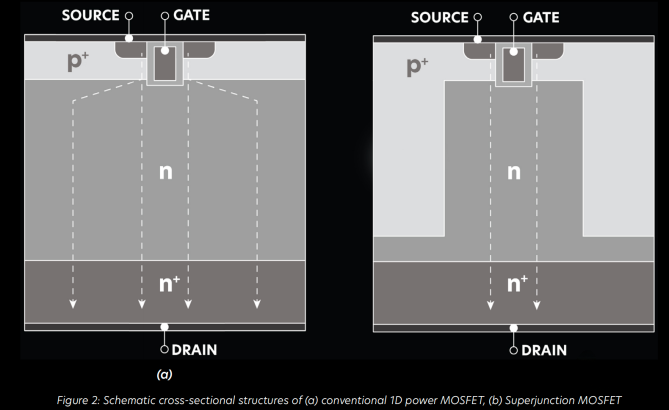
Schematic diagram of the cross-sectional structure of a traditional conventional 1D power MOSFET (a) and a super-junction MOSFET (b) (Source: iDEAL Semiconductor white paper)
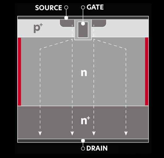
iDEAL's SuperQ structure
(2) Thinner epitaxy: The company's most advanced trench technology, SuperQ, provides near-ideal charge balance, allowing thinner epitaxy and better performance numbers.
(3) Higher doping concentration: SuperQ technology can achieve higher doping concentration in the conduction region due to its blocking efficiency. This increased doping further reduces the resistance of the channel and reduces power loss.
The 200V MOSFET based on SuperQ technology has many advantages: its resistance is 6 times lower than that of existing silicon and 1.6 times lower than that of GaN. Compared with super junction structure, it has 55% larger conduction area; compared with advanced silicon MOSFET driving 36 horsepower motor, it can reduce inverter loss by 46%; motor drive inverter designed with SuperQ technology can save up to 50% power loss.
And SuperQ technology is also expected to be used in "post-silicon" materials. If implemented on other semiconductor materials, it can reshape the cost performance curve of silicon carbide, gallium nitride and other future wide bandgap materials. When the wide bandgap market is mature, SuperQ technology can accelerate its application.
iDEAL CEO Mark Granahan (Mark Granahan) said that their chips may be competitive in 90% of the power chip market. The company has raised $40 million in new funding from investors including the investment arm of semiconductor manufacturing equipment maker Applied Materials.
SiC, the status is not stable
Everyone thought that when SiC would secure its position in some high-voltage markets, GaN would also challenge SiC's position. The material properties of GaN make it an advantageous choice over silicon carbide (SiC) for high-voltage power switching applications. However, GaN processing technology has yet to produce viable GaN high-voltage switching transistors that can operate above 1,000 V. SiC has so far been the preferred broadband semiconductor for 650-1200V applications, especially inverters in electric vehicles and renewable energy. But the development of vertical GaN is becoming a serious competitor to SiC.
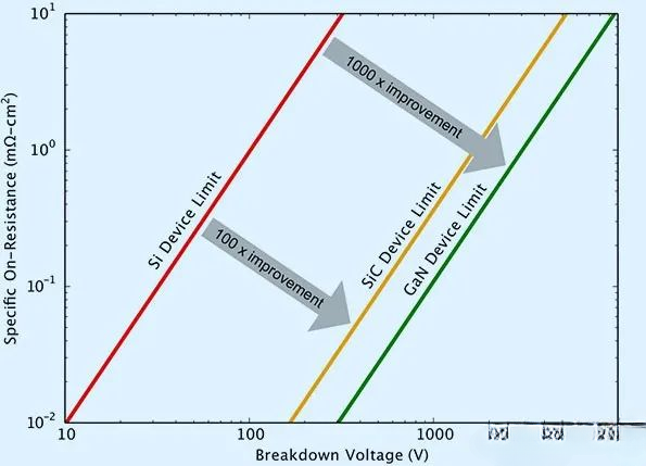
Compare specific on-resistance limits for Si, SiC, and GaN at breakdown voltages of 10-10,000 V.
First of all, it is necessary to popularize science. GaN power devices are mainly divided into "horizontal type" in which GaN active layers are formed on silicon wafers and "vertical type" in which GaN substrates are directly used. The first horizontal type can obtain the high-frequency characteristics of GaN at a lower cost, but it is not suitable for situations that require a high withstand voltage above 650V. The second vertical type is more suitable for high voltage and high current than the horizontal type, but GaN wafers are expensive and small in diameter, about 2 to 4 inches. If the cost problem can be solved, vertical GaN power devices will also have certain advantages.
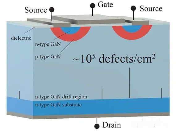
Among vertical GaN R&D players, the first is Odyssey Semiconductor in Ithaca, NY, USA, which has developed a revolutionary approach to achieve area-selectively doped regions in GaN, opening the door to the realization of vertically conductive devices. door. Odyssey Semiconductor is utilizing high-quality bulk GaN wafers as the substrate for its proprietary vertical conduction power switching transistors. These substrates allow the growth of the low defect density device layers required for transistors rated above 1,000 V. GaN grown on Si, according to them, has a defect density of ~108 to 1010 cm². These defects can affect the high-voltage operation reliability of the device. As a result, no GaN HEMTs rated higher than 900 V have been released commercially, and most are limited to 650 V.
Their revolutionary approach has resulted in approximately 1000-10,000 fewer defects per unit area in vertically conducting GaN devices grown on GaN substrates, which will allow reliable operation at voltages up to 10,000 V and beyond. Although GaN substrates are more expensive, GaN devices require much smaller wafer sizes than SiC, making them competitive in production with SiC devices of similar ratings.
It is reported that Odyssey Semiconductor's vertical GaN product samples have been produced, including two working voltages of 650V and 1200V, and will start shipping to customers in the first quarter of 2023. According to reports, the 650V segment is the larger market today and is expected to grow at a CAGR of 20%. The 1200 V product segment is expected to grow faster at a CAGR of 63% and will become a larger market in the second half of the decade. The company's goal is to completely replace the higher power device market currently served by SiC.
Another European consortium interested in vertical GaN, the YESvGaN project, started research in 2021 on a new type of vertical GaN power transistor that achieves the performance of a vertical WGB transistor at a cost comparable to silicon. In the field of power semiconductors, Europe has always had a solid foundation and technology accumulation, and behind this consortium is also a gathering of leading European companies and combinations. The YESvGaN alliance is formed by Bosch, STMicroelectronics, Soitec, Siltronic, AIXTRON, X-FAB and other companies, as well as German research institutions Fraunhofer IISB, Ferdinand, Braun Institute, University of Ghent in Belgium, and University of Valencia in Spain. Established bases in 7 countries Composed of 23 companies/organizations, the European Union's research and development project "ECSEL" JU" and funds provided by European countries.
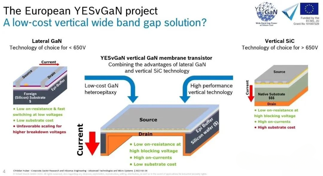
The direction of their research is to obtain cost advantages through the heterogeneous epitaxial growth of GaN on silicon and sapphire substrates, while taking into account the vertical characteristics. Originally GaN on Silicon (the growth of GaN on a silicon substrate) cannot produce a vertical shape because an insulating buffer layer is required. Plus, sapphire itself is an insulator. Therefore, this project removes the buffer layer directly under the device region after GaN growth and the silicon and sapphire substrate itself, and directly connects to the GaN layer through metal contacts from the back, which is called a "vertical GaN thin film transistor". The current development goal of this project is to use 300mm silicon or sapphire wafers to manufacture vertical GaN power transistors with a withstand voltage of 650 ~ 1200V. Although the thickness is only a few microns, the advantages of the vertical structure are similar to those of GaN on Silicon or GaN on Sapphire's low cost will be possible.
The figure below shows some of the main research steps and work to be done for YESvGaN, mainly including: 1) In order to achieve 650 ~ 1200v level, the technology development of thick drift layer epitaxial growth on a silicon/sapphire substrate of *300mm; 2) *1200V/100A on-resistance 4mΩcm² vertical GaN power transistor development and process technology with the same cost as silicon IGBT; 3) Remove the silicon substrate and buffer layer by dry etching, and form the elevation and settlement of the sapphire substrate by laser lift-off Contact, and backside power element fixing technology through advanced bonding and mud strips; 4) Development of power transistor components and interconnection technologies, as well as corresponding reliability characteristic evaluation; 5) Create data sheets for the developed power transistors System efficiency improvements are demonstrated in multiple application demo machines.
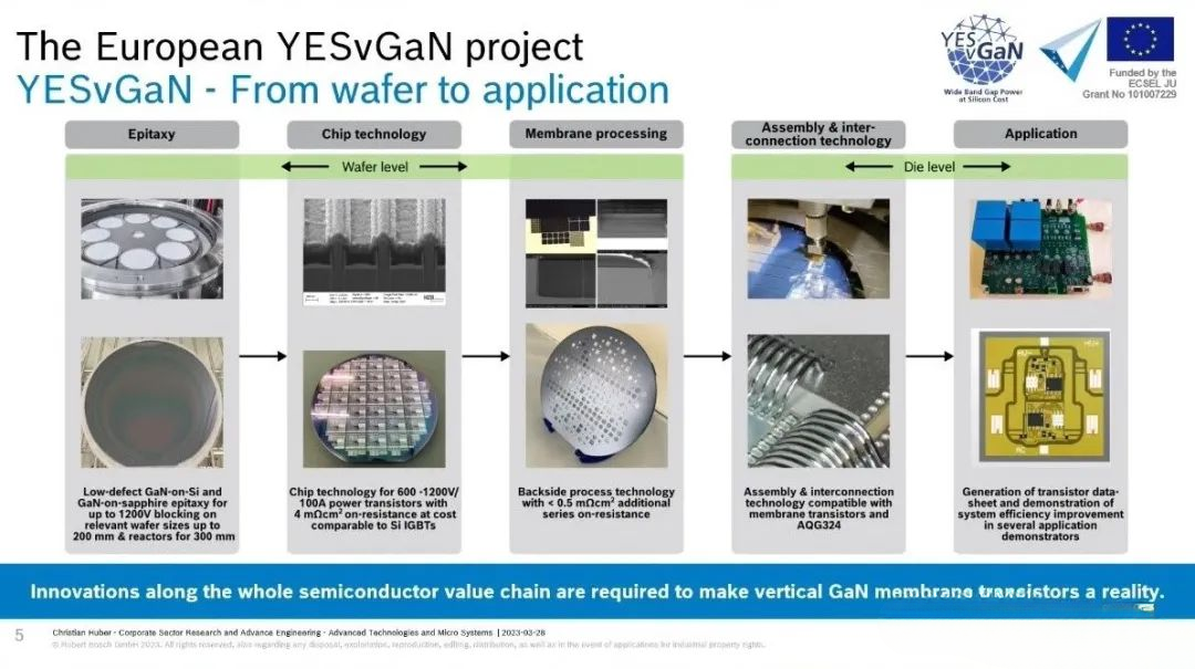
At the world's largest power electronics exhibition PCIM Europe 2023 (May 9-12, 2023, Germany), Bosch is presenting the progress of its YESvGaN project, which has achieved diode growth on silicon and sapphire with a breakdown voltage of over 500V. stacked layers, and silicon was removed on a 150mm GaN on Silicon wafer to form a 4μm thick GaN film with a maximum diameter of 5mm. However, Bosch has not yet reached the stage of final transistor completion, and is currently conducting a lot of research around verifying whether the technology is feasible. If this technology is realized, it is expected to accelerate the mass production of vertical GaN.
150mm GaN on Silicon wafers from Bosch at PCIM Europe 2023
In addition to this, the Belgian research laboratory imec demonstrated a breakthrough Gallium Nitride (GaN) process on 200mm wafers. In cooperation with Aixtron's equipment, imec has demonstrated the epitaxial growth of GaN buffer layers for 1200V lateral transistor application on 200mm QST substrate with hard breakdown voltage over 1800V.
In short, the research and development of vertical GaN is also a major direction of industry efforts. These enterprises and institutions are working hard to develop and tap the potential of GaN under high voltage.
New materials, the future can be expected
In addition to efforts on silicon, SiC and GaN. New power semiconductor materials such as gallium oxide and diamond are also the direction that the industry is tackling. In the exploration of new materials, Japan has always been in a leading position. Many companies in Japan have rich production performance in the fields of power semiconductors and high-frequency components.
Diamond is far superior to semiconductor materials such as SiC and GaN in terms of band gap, electron mobility, thermal conductivity, etc., and is also known as the "superior semiconductor material". Not only semiconductors, diamonds can also be applied to quantum sensors.
Japanese companies such as EDP Co., Ltd. and Orbray Co., Ltd. in Japan are actively promoting the wafer business of diamond materials. Among them, "Orbray" has developed a production method of Heteroepitaxial Growth (Heteroepitaxial Growth) diamond wafers using sapphire as a substrate, and has now successfully produced wafers with a diameter of 2 inches.
In addition, the Japanese start-up company Waseda University hatched a start-up company Power Diamond Systems with the business goal of "realizing the practical use of diamond semiconductors", intending to push the research and development achievements of Professor Kawaharada, a pioneer in the diamond semiconductor industry, to practical use. Professor Kawaharada used the basic technology of diamond semiconductor (hydrogen terminal surface) to develop diamond field effect transistor (FET), which is well known in the industry.
The report of the Japan Electronic Equipment Industry News pointed out that diamond semiconductors have begun to move from the laboratory to practical application. However, it will still take a long time to popularize and promote the application of diamond semiconductors. However, reports have pointed out that within a few years at the earliest, there will be prototypes of diamond-made semiconductors.
As more and more Japanese companies and university institutions explore new materials such as diamond and gallium oxide. It is believed that it will provide more development space for the development of power semiconductor devices in the future.
Another material with great potential is gallium oxide. With its wide bandgap close to 5 electron volts, gallium oxide*GaN (3.4eV) is one mile away. Compared with silicon (1.1eV), the absolute advantage is as large as a marathon . Among the five properties that are critical to semiconductors, high critical electric field strength is the biggest advantage of β-gallium oxide. Gallium oxide can also be made more conductive through a process called doping. This helps create high-voltage switches, and could mean powerful RF devices can be designed based on them.
In April 2023, Novel Crystal Technology in Japan is working on the commercial development of β-Ga2O3 Schottky barrier diodes. Under the impetus of Japan's New Energy Industry Technology Development Organization (NEDO), it has also successfully demonstrated the introduction of a trench structure (Trench Structure) with a withstand voltage of 1,200V and a low-power Gallium Oxide Schottky diode.
As early as 2021, Novel Crystal Technology successfully mass-produced 4-inch gallium oxide wafers, and has begun to supply customer wafers this year. In addition, Novel Crystal Technology also plans to supply 6-inch wafers in 2023. In 2021, Novel Crystal Technology plans to invest approximately 2 billion yen to add equipment to its company factory, and by 2025, build a production line with an annual output of 20,000 100mm (4-inch) gallium oxide (Ga2O3) wafers.
Regarding the research and development of gallium oxide, domestic breakthroughs have also been made. On March 14, Xi'an University of Posts and Telecommunications announced that the team of Professor Chen Haifeng of the school had successfully prepared high-quality gallium oxide (GaO) epitaxial wafers on 8-inch silicon wafers; CETC) announced that CETC 46 successfully prepared my country's first 6-inch gallium oxide single crystal, reaching the highest international level.
Epilogue
Whether it is the structural innovation of existing silicon-based power semiconductors, the breakthrough of vertical GaN, or the exploration of newer materials such as diamond and oxide grafts, it is all aimed at providing better solutions for the industry. With the continuous advancement of technology and the growth of demand, breakthroughs in power semiconductors will bring about tremendous changes and improvements in electronic equipment and energy systems.
In general, the development prospects of power semiconductors are very exciting under the continuous breakthrough of new materials and new structure technologies.
References for this article:
Diamond semiconductors are beginning to be practical, Japan Electronics Industry News


 English


