Chiplets, a big step forward
Chiplets, a big step forward
In recent years, Chiplet has become the next key innovation stage in the chip industry, and is a technology choice that continues the "Moore's Law".
AMD, TSMC, Intel, Marvell and other chip giants with a strong sense of smell and strong technical strength, have entered the game. Chiplet Under the new track, from these chip giants are fighting for themselves, to the industry standardization "close", everywhere undercurrent surging.
Is mediatek's recent reventure with Nvidia, Jim Keller and LG an important step forward for Chiplet? How far further is the dream of a "small chip store"?
1. Why does Chiplet stand on the tuyere?
At present, with the continuous evolution of chip process nodes, the problems of heating and leakage caused by short channel effect and quantum tunneling effect are becoming more and more serious, and the "Moore's Law" in pursuit of economic efficiency is slowing down.
The high cost of chip development and manufacturing under the advanced manufacturing process also brings huge cost pressure and investment risk to Fabless companies, which forces people to seek more cost-effective technology routes to meet the industry's growing demand for chip performance.
In this context, the industry began to turn to a new track represented by advanced packaging, along with advanced packaging and the emergence of a new concept is Chiplet, also known as the core or small chip in the industry.
Traditionally, to develop complex SoC products, vendors need to design a chip that integrates all functions on the same chip. In each subsequent generation, the number of functions of the chip increased dramatically, especially at the latest 7nm, 5nm, 3nm nodes, where the cost and complexity soared.
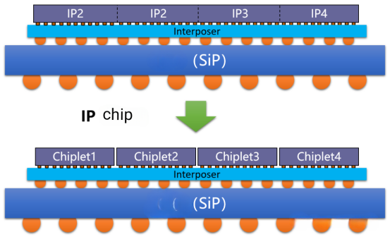
And the principle of Chiplet is originally a complex SoC chip, from the design according to the different computing unit or functional unit decomposition, then each unit choose the most suitable process manufacturing, then the modular bare interconnection, through advanced packaging technology, different functions, different process manufacturing Chiplet package into a SoC chip.

Because the decomposed core particles can be separated and manufactured, different processes can be used. For modules sensitive to process improvement, such as CPU, advanced process can be used, while for modules not sensitive to process improvement, such as IO, mature process with low cost can be used, so as to reduce the cost.
To put it simply, Chiplet aims to "integrate large chips into pieces". Single Chip is essentially IP hardware-based, and Chiplet package can be regarded as the integration of multiple hardware-based IP. For the subsequent upgrade of Chiplet chip, only the Chip corresponding to some IP units can be upgraded, and some IP can be retained by —— to realize a new form of IP reuse, which can not only obtain lower cost with the help of production scale, but also greatly shorten the product launch cycle.
According to Omdia, the Chiplet market is expected to reach $5.8 billion by 2024 and exceed $57 billion by 2035, with rapid growth.
2, UCIe, looks together
While the above sounds ideal, the individual naked films vary greatly in bandwidth, interoperability, and data integrity, and only the big companies have the resources to support customized interconnect development.
From the perspective of Chiplet market progress, AMD, TSMC, Intel, Nvidia and other chip giants smell the market opportunity in this field, and began to enter the Chiplet in recent years.
AMD products have greatly benefited from the "SiP + Chiplet" heterogeneous system integration mode; Intel launched its * Sapphire Rapids, a fourth-generation to strong scalable server processor based on Chiplet design; Apple's released M1 Ultra chip, Interconnect of the two M1 Max chips through the Chiplet package scheme, To achieve higher performance and more economical solutions; Marvell Since 2016, Chiplet has been used to design its network processing and communication chips; Intel Foundry Services Customizing the system for core-based data center customers...
The dynamics and layout of technology giants all reflect that Chiplet technology is being recognized and valued in the industry. Chiplet It has become a technology choice for chip manufacturers to enter the next critical stage of innovation and break the power-performance-area (PPA) ceiling.
However, although there are many advantages, Chiplet, like all new technologies, faces many challenges, limited by different interconnect interfaces and protocols produced by different architectures and manufacturers. Designers must take into account many complex factors such as process, packaging technology, system integration, and extensions. At the same time, it also meets the requirements of different fields and different scenarios for information transmission speed and power consumption, making the design process of Chiplet extremely difficult.
Chiplet Whether it can become a new IP product and business model, or even save the savior of Moore's Law, the key is whether the industry can achieve a unified Chiplet interconnection standard and establish an open and standardized Chiplet ecology.
From the above Chiplet technology manufacturers, all these companies rely on the internal core ore to achieve, is essentially decomposed SoC.
In this process, many chip manufacturers are pushing their own interconnection standards, such as Marvell using Kandou bus interface when introducing modular chip architecture; Nvidia's high-speed interconnection NV Link scheme for GPU; Intel authorized AIB advanced interface bus protocol for free; LIPINCON protocol launched by TSMC and Arm; AMD also has Infinity Fabrie bus interconnection technology, and HBM interface for memory chip stacking and interconnection.
As you can see, these chip giants are actively exploring Chiplet technology, but at the same time, they are fighting separately to promote their own high-speed interconnection protocol standards. Some industry experts point out that there is no unified communication interface between different processes, functions and packaged chips, which will cause a serious waste of resources.
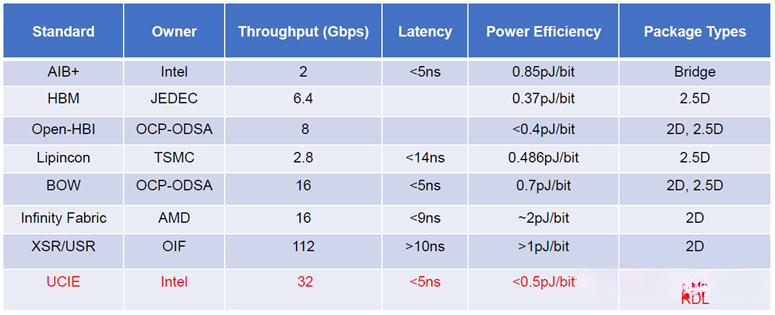
Some existing interconnection standards on the market are compared as follows:

Among the current Chiplet interconnection standards, BoW initiated by the Open Computing Project (OCP) and UCIe proposed by Intel have attracted the active participation and investment of many leading enterprises in the high-tech field.
BoW, full name Bunch of Wires, is a suitable for Chiplet and chip level package interconnected simple physical interface architecture, at first for data center computing, communication and network requirements of short distance interconnection solutions, later by OCP subordinate open specific domain architecture (ODSA) working group adopted for connect the same package close bare interconnected interface protocol.
Different from the interconnection between server boards, the interconnection environment of multiple bare chips in the chip package is relatively stable. Because the distance is short and the signal attenuation is small, so the interconnection design can be relatively simple. In fact, the original intention of BoW interface design is to achieve low implementation cost, compatible with different IC process nodes, and can flexibly support a variety of packaging technology convex and concave spacing, so as to meet the requirements of low power consumption, low latency and high throughput of complex chips.
According to OCP / ODSA, BoW has the following advantages when applied to Chiplet interconnection:
Higher data rate than the existing parallel standards;
Suitable for traditional low-cost laminate substrate packaging and higher density silicon interposer packaging;
It is easier to achieve than using the traditional SerDes link design;
Compatible with the packaging case of mixed convex and concave spacing.
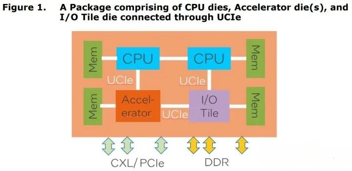
In addition, the universal Chiplet Interconnection Standard (UCIe) proposed by Intel has attracted wide attention in the industry in a very short time. UCIe "UniversalChiplet Interconnect Express" aims to establish a unified standard for connectivity at the chip packaging level to help build an open small chip ecosystem across the entire semiconductor industry.
UCIe is a hierarchical protocol that specifies the physical layer, the die-to-die adaptation layer, and the protocol layer:
Uptop protocol layer: ensures * efficiency and * delay through a protocol based on the flow control unit (FLIT), and supports multiple mainstream protocols, including PCIe, CXL, and user-defined flow protocols.
D2D adaptation layer in the middle: used for arbitration and negotiation of the agreement, and connection management through the bare tablet adapter. This layer also includes an optional error correction function based on cyclic redundancy check (CRC) and retry mechanism.
Lower physical layer (PHY): Specifying the electrical interface with the packaging medium is the level of parameter exchange and negotiation of the electrical / analog front end (AFE), transmitter / receiver and sidebchannel between the two bare plates. Logical PHY enables connection initialization, training and calibration algorithms, as well as test and repair capabilities.
The impact of the launch of UCIe standards on the industry is to promote Chiplet from "talk" to "practice", from "each family" to "team fighting". The giants are working together to build a unified Chiplet interconnection standard, allowing end users to build SoC chips with small chip parts from multiple vendor ecosystems, which will accelerate the development of an open Chiplet platform and span x86, Arm, RISC-V and other architectures and instruction sets.
As mentioned above, almost all of these small chip based designs have in common is that they are done in one company. But ideally, everyone wants to be able to take their supermarket cart to a small chip store (Chiplet store), pick the small chips they want from the shelf, and then be able to assemble a system-level package (SiP) to work.
With the gradual development of Chiplet, the interconnection demand between core particles from different manufacturers may continue to increase in the future. Therefore, before the technology matures and the business trend forms, the industry manufacturers need to build a "bridge" of Chiplet interconnection interface standardization.
However, from the current situation of the industry, neither BoW nor UCIe seem to have been able to assume the role of this "bridge", and the dream of small chip stores is still far away.
In this regard, Associate Professor Huang Lotte of the University of Electronic Science and Technology told the semiconductor industry observation that, on the one hand, the UCIe standard was initially proposed and formulated by Intel, and then opened to the industry to form an alliance. But in the UCIe standard Intel background is too heavy, similar to Intel do a complete set of solutions, others according to Intel open accelerator interface, UCIe interface do the remaining 20% of the work, Intel want to be "Chiplet" Arm, or in Chiplet era reshaping PC era X86 processor + chipset + peripheral board card mode. It tries to form a heterogeneous accelerator Chiplet design ecology outside the basic system of its core processors, and attract special accelerators or field special processors designed by other manufacturers to integrate with the Chiplet-form CPU ecosystem in the form of Chiplet.
On the other hand, the launch of UCIe is not *, at least part of the problem is that the interconnect standards are never really done. Associate Professor Huang Lotte said that UCIe is currently positioned to connect the accelerator, IO Die and other Chiplet, which is similar to the Chiplet version of the PCIe interface. The Chiplet system has not only the accelerator and IO Die, the core between the main processor and the main processor, and the connection between the main processor and the memory is not within the view of UCIe. At the same time, the data interaction and interoperation between Chiplet require a complete set of protocol stack, and much of the content is not specified in UCIe. Instead, there is a complete solution in the CXL standard, which Intel recently highlighted. CXL can be used for more advanced low-latency / high-throughput connections, such as memory, I / O, and accelerators, caches such as GPU and ASIC. UCIe is more like a model for being compatible and supporting CXL in the Chiplet era.

Therefore, in this model and attempt, although UCIe has substantial manufacturer involvement. However, manufacturers will not devote themselves to the existing standards, but will put a large part of their energy on establishing a new agreement standard around their products and technologies, and strive to create their own small ecology, forming a situation of "occupying the mountain is king".
For example, Mediatek recently announced that it will develop a vehicle SoC integrating Nvidia GPU core particles, equipped with Nvidia AI and graphics computing IP. The core particles support interconnection technology, which can realize smooth and high-speed interconnection between core particles. And Jim Keller's companies Tenstorrent and LG announced that they are working together to build a new generation of RISC-V architecture AI and video codec Chiplet to potentially power LG's future high-end TV and automotive products.
These two partnerships are undoubtedly the attempt and exploration of industry manufacturers in the third-party core particle suppliers, releasing a signal that the industry is actively exploring around their respective standards. The dream of a small chip store seems to be a step closer.
In general, there are inevitably multiple technical routes in the current development of Chiplet, and how to define a standardized protocol that is mutually recognized in an industry is very complex. At least there is no interconnection standard and technology that can meet the industry's "universal" needs.
Looking ahead, whoever leads the lead in Chiplet business is likely to dominate industry standards. Huang Lotte said that many industry standards and agreements are not formulated by everyone together, and the coexistence of multiple standards ultimately depends on the winner as the king. That is, who can stand out in the "chaotic times", who can be the first in the business competition is the standard.
However, in contrast, domestic companies have made slower progress in Chiplet. Huang Lotte divides the Chiplet into three stages:
In order to reduce costs and improve the yield, the large chip is cut small;
The enterprise forms internal core serialization, internal IP reuse, in the form of series of products to do set reuse;
Through the accumulation of core particles, the general purpose of core particles between different manufacturers is realized, and a perfect design methodology and process are formed.
However, the reason why the domestic development is slow is that almost all local enterprises have no ability to achieve the second stage, so they want to directly match the third stage of foreign manufacturers to achieve the vision that the industry giants have not realized. Although the third stage is of great significance to alleviate the current difficulties facing our country, it is not advisable to encourage the seedling. Domestic manufacturers also need to be patient down the step by step to finish the journey.
Therefore, Huang Letian suggested that domestic practitioners do more practical work and less shout slogans, talk less about ideas and do more practice, and first walk out of a way. If you want to "overtake on the curve", you must dare to make up your mind to make a large investment, and support the domestic head enterprises to form a business alliance with industrialization ability to achieve a breakthrough.
3. Beyond the connectivity standards, the Chiplet still faces many challenges
Solving the interconnection standard is just a * step forward. At the technical level, Chiplet also faces challenges from chip testing, software coordination, and responsibility division.
Chip testing: For Chiplet, splitting a large SoC chip into multiple core particles is more difficult than testing a complete chip, especially when testing some Chiplet's that do not have independent functions. Therefore, it is very important to test each chip thoroughly before it goes into the assembly process. These naked films are called KGD, or Known Good Die.
Some industry experts say that with the current chip complexity and more complex packaging, the need to test the technology, which is like closing your eyes and running in the forest, will be very difficult. The test of many cores needs to be completed in the wafer stage, which requires more probes to complete the test simultaneously. Especially for 3 DIC, it is a "black box" inside, and the test probe can only obtain a limited amount of data through some points on the surface, which also brings great challenges to the analysis and test of 3 DIC. At the same time, in order to improve the overall yield after sealing, Chiplet integration also puts forward higher requirements for testing and quality control, including signal quality verification of interconnection lines, interoperability function verification, test coverage and other considerations, etc. In addition, it also poses higher challenges to the finished FT test process and test equipment after sealing of wafer level CP and Chiplet.
System design complexity: For chip design, although there is no need to design complex large chips, integrating SoC into Chiplet and integrating it into a 2.5D / 3D-package will bring a significant increase in the system complexity, and there are great challenges in system design. Compared with the original 2D single chip, Chiplet is combined with 2.5D / 3D package, and its internal core may adopt different manufacturing processes and different architectures. At the same time, it also needs to add high-speed interconnection bus, interface IP and HBM memory, and each module may also need to use different materials for interconnection. Therefore, in the chip design, it is necessary to regard the internal packaged modules as a whole system, and the design and optimization of the whole system level should be taken into account at the beginning.
EDA tools and other software cooperation: the design and manufacturing of Chiplet requires EDA software support from architecture to implementation and then to physical design. In addition, the management and invocation of each Chiplet also need unified standards in the industry. Currently, the Chiplet technology lacks a relevant EDA tool chain, as well as a complete and sustainable ecosystem.
Accountability and security: Commercial small chips add another thorny question: who is responsible when accidents or errors are observed? Or is it not a small chip problem, but what happens if the substrate or physical interconnection is defective? One vendor trusts the processes of another. Small chips coming from different processes will have different thermal expansion coefficients, thus leading to thermal stress or mechanical reliability problems.
Chiplet Technology faces a variety of interactive challenges, like a "whack-a-mole" game, with one problem solved, it will bring about another field of problems.
In addition to the technical challenges, uncertain factors such as the unclear division of labor of Chiplet and the positive cycle of economies of scale may also lead to the shortage of the supply side and the lack of stable and diversified Chiplet supply. Under multiple troubles, the Chiplet industry needs to work together to build ecological prosperity.
Despite the challenges, the future of Chiplet still seems promising in terms of the dynamics and layout of industry vendors.
Write at the end
Chiplet The development and rise of technology is not only the need of technological development, but also the drive of economic laws.
Even more attractive, building the Chiplet ecosystem is expected to address the current "insect paradox" facing the chip industry.
Insect paradox refers to that the current Internet of Things, artificial intelligence and other applications may be as numerous as insects, but the number of single applications is small, and the current hardware design tends to be specialized, making it difficult for the "slow and expensive" traditional chip design method to share the cost through the way of volume. Through decomposition means, Chiplet decouples the CPU, accelerator and other resources in SoC, and even divides the same resources into more fine-grained modules, so that Chiplet can be reused in a variety of designs. In the Chiplet ecosystem, users can choose the core particles from the cores provided by various suppliers according to their own needs, and then combine them into a personalized system.
In short, the chip industry is actively exploring Chiplet technology to balance the contradiction between rising R & D spending and lower shipments.
Looking around the moment, even though the Chiplet industry is still full of challenges, the difficulties will always be overcome, and the market will eventually move from disorder to the right track.


 English


