DRAM, accelerating towards 3D
DRAM, accelerating towards 3D
"Especially as the 10nm process approaches, it defines the circuit pattern on the wafer close to the limits of basic physics. The scaling of DRAM memory cells is slowing due to challenges in process integrity, cost, cell leakage, capacitance, refresh management, and sensing margins."The Techinsights analyst added. So, as the report says, the industry is looking for new solutions.
French analyst Yole also points out that even with the lithography EUV process, plane scaling is not enough to provide the required bit density improvement throughout the next decade. Therefore, we urgently need breakthroughs in materials and architecture to further expand DRAM to reduce costs, limit power consumption and increase speed. Monolithic 3D DRAM (equivalent to 3D NAND of DRAM) has been seen as a potential solution for long-term expansion by major equipment suppliers and DRAM manufacturers.
According to Yole's estimate, the novel 3D technology could hit the market within the 2029-2030 time range. South Korean media businesskorea stressed that three DRAM giants, including Samsung, SK Hynix and Micron, are accelerating the commercialization of 3D DRAM.
Why is it a 3D DRAM?
The so-called 3D DRAM is a memory chip with a new structure that breaks the current old paradigm.
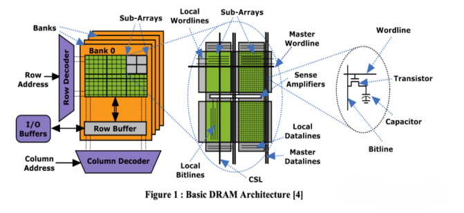
As shown in the figure below, the conventional DRAM is organized as a set of storage bodies that includes storage elements arranged in rows and arrays. Memory arrays are grouped in a hierarchical structure of memory subarrays for efficient wiring and reduced power consumption. Each storage cell is modeled as a transistor capacitor pair, and the data is stored in the capacitor as a charge. The individual units in each subarray are also connected to the local word line and the local status line. This micro-one-capacitor-one-transistor design makes it ideal for packaging large numbers of storage units into small areas to achieve high density and high storage capacity. In fact, there are billions of DRAM units that can be compressed onto a single memory chip.

However, in traditional DRAM manufacturing, the industry almost always uses the DRAM stacked in the same plane to produce DRAM, and chip manufacturers improve the performance of DRAM by reducing the unit size or spacing. However, they reached the physical limit of increasing the number of cells within a finite space. Another problem is that if capacitors get thinner, they can collapse.
Therefore, 3D DRAM, which developed from high altitude like 3D NAND Flash, became the target.
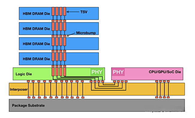
According to a report by semiengineering, there are two paths to DRAM in 3D, and the most direct way is to keep current DRAM technology and stack multiple chips on top of each other. This is an advanced packaging method for high-bandwidth memory (HBM). Common HBM, with chip 4 and 8 high, is expected to reach 16 highs soon. This is a more expensive approach compared to basic DRAM because of the effort required to stack a die in a package, but it is worthwhile for applications that require a lot of nearby memory (such as AI).

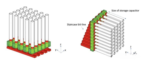
In addition to this method, single chip stacked DRAM is another option, I believe this is the ultimate goal of all manufacturers. As a natural extension, a single olithic stacked chip requires only a few extra steps, but this small extra step can cause many difficulties. In order to achieve this goal, some analysts believe that 3D DRAM can follow 3D NAND Flash and turn cell over. Because the DRAM unit has a small 2D region but a large vertical direction capacitor, it makes it high and difficult to stack in layers. Moreover, as the 2D size gets smaller and the capacitor gets thinner, it must be lengthened to maintain sufficient charge.
However, if it is flipped to one side and rotated 90 degrees, the cells can be layered using the ladder design of each line. In this way, the lithographic patterned process for making the layers during the DRAM manufacturing process can be used for all layers —— The so-called shared patterned —— which simplifies the manufacturing process.

At the same time, researchers began to explore capacitive 3D DRAM, including Dynamic Flash Memory, VLT, Z-RAM and IGZO-FET. But from the current news, the three storage giants (Samsung, SK Hynix and Micron) have not disclosed more details.
But there is no doubt that this is all their way forward.
The giants keep their down
In an interview with semiengineering in 2021, none of the three storage giants responded to anything about their 3D DRAM solution. But Yole reported in early 2022 that Samsung Electronics was preparing to develop the world's * 3D DRAM, and was accelerating the development of the 3D DRAM.
According to Yole, Samsung Electronics has begun developing a technology for stacking cells, a stacking concept quite different from high-bandwidth memory (HBM). In addition, Samsung Electronics is also considering adding the contact surface between the gate (current gate) and the channel (current path) of the DRAM transistors. This means that the three-side contact FinFet technology and the four-side contact ring gate (GAA) technology can be used for DRAM production. The transistor can control the current more precisely as the contact surface between the gate and the channel increases.
In an interview with eetimes in September 2022, Micron also confirmed that it was exploring a 3D DARM solution.
Micron says the 3D DRAM is being discussed as the next step to continue to extend DRAM. In order to achieve 3D DRAM, the entire industry is actively doing research, from the development of manufacturing equipment, advanced ALD (atomic layer deposition), selective vapor deposition, selective etching, to architecture discussion.
Micron also stressed that the main problems with the 3D DRAM are still in terms of cost and technology. Technical challenges exist in a wide range of areas, including equipment and structures, manufacturing processes, manufacturing equipment, materials, and architectures."In order to move from flat DRAM to 3D DRAM, innovation in all areas is needed. Furthermore, this transition needs to be implemented where the cost curve and performance intersect with the DRAM scaling roadmap."The Micron side emphasized.
To that end, Micron admits that the industry continues to expand flat and look for ways to advance the DRAM roadmap. In addition, the development of new memory architectures is ongoing, so the role of DRAM in the system is changing, perhaps potentially to maintain planar over a longer time."At this point, memory manufacturers are investing (flat and 3D) to expect inflection points to sustain DRAM expansion, and while each node expansion of DRAM is becoming increasingly difficult, the traditional expansion will continue, at least over the next few years."Micron continued.
Yole said Micron had filed a 3D DRAM patent application that is different from Samsung Electronics. Micron's approach is to change the shape of the transistors and capacitor without placing cells.
As for SK Hynix's 3D DRAM plan, there is not much introduction online. But Yole stressed that SK Hynix is investing heavily. In addition, global semiconductor equipment manufacturers such as Applied Materials and Lam Research are also starting developing solutions related to 3D DRAM.
According to the three storage giants in 3D DRAM, according to businesskorea citing TechInsights data, Micron has been working on 3D DRAM research since 2019, obtaining two to three times the number of patents than the two South Korean chip makers.
TechInsights It further noted that Micron, which ranks third in the memory semiconductor market, is actively preparing for the blue ocean market and will receive more than 30 3D DRAM patented technologies by August 2022. By comparison, Samsung has fewer than 15 3D DRAM patents, while SK Hynix holds about 10 patents.
In addition, many domestic research institutions and even enterprises are investing in the research and development of 3D DRAM. Microelectronics of the Chinese Academy of Sciences has said, in view of the density of IGZO-DRAM, microelectronics key laboratory of microelectronics liu Ming team in vertical ring channel structure (Channel-All-Around, CAA) IGZO FET, studied the influence of the second device stack before interlayer process, verify the reliability of CAA IGZO FET in 2T0C DARM applications.
Write at the end
As Micron said earlier, there is still a lot of uncertainty about the future of the 3D DRAM, and Yole even thinks the technology won't come until 2029 or 2030.
Another analyst, Techinsights, said that if current DRAM manufacturers maintain the 6F2 DRAMcell design of 1T + 1C structure, the 10nm D / R unveiled in 2027 or 2028 will be the last generation of new DRAM technology. DTRAM unit scaling will face challenges such as 3D DRAM, row hammer scaling (circuit), low power design, refresh time scaling (refresh time scaling) and management, process challenges like low latency, new work-function materials, HKMG transistors and on-chip ECC. For details, please refer to the semiconductor industry observation in the previous article.
The imec notes that emerging memory, including resistive RAM, magnetic memory (like MRAM), phase change memory (PCM), and ferroelectric memory, has been studied to replace classical memory and storage solutions (static RAM (SRAM), DRAM, and NAND-Flash), or to fill the gap between the fast and expensive DRAM and slow and inexpensive NAND (so-called storage memory).
"However, most emerging memory is difficult to adopt in the market. This has led memory companies to refocus on expanding DRAM and storing NAND flash —— to meet traditional density requirements."imec try to persuade.
In other words, for DRAM manufacturers, exploring how to increase the density will be the direction that they need to work on for a long time.


 English


