who invented the transistor?
who invented the transistor?
In the early 20th century, scientists knew how to make diodes at both ends by contacting sharp metal probes with semiconductor crystals. These point-contact diodes can turn oscillating signals into stable signals and are widely used as detectors in crystal radio receivers. By the 1920s, inventors began studying the use of semiconductors to amplify and switch signals.
Some of the earliest semiconductor amplifiers worked were from Eastern Europe. In 1922-23, Russian engineer Oleg Losev at the Nizhegorod Radio Laboratory in Leningrad, found that a special working mode of point contact zinc ore (ZnO) crystal diodes supported signal amplification of up to 5 MHz. Although Losev had experimented with this material in radio circuits for many years, he died during the Siege of Leningrad in 1942, unable to justify his place in history, so his work is largely unknown.
The Austro-Hungarian physicist Julius E. Lilienfeld Moved to the United States and in 1926 filed a patent for "methods and devices for controlling current control," in which he described a three-electrode amplifier using copper sulfide semiconductor material. Lilienfeld Is believed to have invented the electrolytic capacitor, but there is no evidence that he made a working amplifier. However, his patent bears enough similarity to later field-effect transistors to reject a future patent application for the structure.
The German scientists also contributed to this early study. In 1934, while working at the University of Cambridge, German electrical engineer and inventor Oskar Heil applied for a patent for which the current —— in the semiconductor is essentially a field-effect transior through capacitive coupling on the electrode.
In 1938, Robert Boer (Robert Pohl) and Rudolf Helsch (Rudolf Hilsch) tested the potassium bromide crystals with three electrodes at the University of Gottingen. They reported an amplification of the low-frequency (about 1 Hz) signal. None of these studies bring any applications, but Heil is remembered in today's enthusiast circles for its air-motion transformer used in high-fidelity speakers.
Gifted Shawkley
Because of its poor reliability and high power consumption, AT & T engineers in the late 1930s knew that vacuum tube circuits could not meet the company's rapid growth in telephone capacity. Research Director at the Bell Laboratory, Mervin J. Kelly Assign William Shockley to study the possibility of using semiconductor technology to replace electronic tubes.
In early 1945, Shockley used improved semiconductor materials developed for radar detectors during the War to test with a field effect amplifier with concepts similar to Heil and Lilienfeld patents, but failed to work as he wished. Physicist John Badin (John Bardeen) has suggested that electrons on the semiconductor surface may prevent electric fields from penetrating into the material.
Under the Shockley, Bardeen began with physicist Walter Brattain to study the behavior of these "surface states".
Walter Houser Brattain (1902-1987) followed his parents in a ranch near Tonasket, Washington. He received his master's degree from the University of Oregon and his PhD from the University of Minnesota. Brattain joined Bell Labs in 1929 as a research physicist, where he was regarded as a skilled experimenter.
Theoretical physicist John Badin, John Bardeen (1908-1991), born in Madison, Wisconsin, jumped his third grade in school as a child prodigy. He earned his master's degree from the University of Wisconsin and his PhD from Princeton University, where he developed an interest in solid-state physics.
Under the secret code name "The Surface State Job," their project is a key priority for AT & T research firm Bell Laboratory to find smaller, lower-power alternatives to bulky, power-hungry vacuum tubes. Research Director of the laboratory Mervin J. Kelly Thought that crystalline semiconductor materials, such as germanium or silicon, may provide solutions. To that end, in 1936, he recruited William Shockley from the Massachusetts Institute of Technology (MIT) to study solids.
William Bradford Shockley Born in London, England, to American parents, he spent his youth in Palo Alto, California, just a few yards from the famous HP garage. As a precocious child, he is "irritable, spoiled and barely uncontrollable, making the life of his doting parents miserable". He received a bachelor's degree from the California Institute of Technology and a doctorate in theoretical physics at MIT. Gordon Moore, a talented Intel company, commented that Shockley "can see electronics", but Shockley was conceited and capricious, so while he had the support of management, he was not very popular with his peers. Nobel Prize winner Charles Townes is even more blunt: " He knows everything, but he doesn't understand people.”
In 1939, when Shockley was convinced that he could find a solution based on solid materials, he wrote: " Today I think that, in principle, amplifiers could be made using semiconductors rather than vacuum rollers."Brattain assisted Shockley in experimenting with what we call today a field-effect transistors (FET) idea, but achieved no useful results.
But the ensuing World War II disrupted the work, but it resumed in 1945 when Shockley hired John Barding and asked him to see if he could see something wrong with his design. Bardeen Initially concluded that it should work.
A FET is a device that uses an electric field to control the current flow in a semiconductor material. Shockley published a paper in the MIT era assuming that electrons near the surface could move as freely as electrons in the body of the material. On March 19,1946, Badin theoretically determined that this claim did not stand. He concluded that the electrons in the region must be captured to create a surface state that forms a movement disorder.
Bardeen and Brattain, with the help of physicist Gerald Pearson and chemist Robert Gibney, work to finding out if he is right. By early 1947, in laboratory experiments, they had demonstrated the presence of a barrier. As their manager, Shockley would make advice on how to break barriers, but not involved in their daily work.
Fantastic November
On Monday, 17 November, Gibney recommended that Brattain apply a voltage between the metal plate on the upper surface and the contacts on the back of the Ge crystal plate to generate a strong electric field perpendicular to the surface. A drop of liquid electrolyte in the material neutralizes the surface state and produces a measurable field effect in the structure.
Following Bardeen recommendations to probe the surface with a sharp metal spot surrounded by an electrolyte, on November 21, Brattain made a functional amplifier, albeit at a very low frequency. During what Shockley calls "Magic Month," weeks of long and fanatical activity on the chalkboard and lab bench, combining accidental "accidents" of handling materials and clever intuition, using what they had learned in the absence of electrolyte presence.
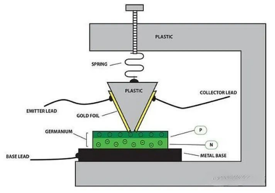
Bardeen Calculates that reducing the distance between the two contacts enhances the effect. Brattain Conted an ingenious method of attaching the gold foil to a plastic wedge and then surgically cutting the tip precisely with a razor blade to create two contact points separated by the width of a sheet of paper.
On Tuesday afternoon, December 16,1947, they connected a spring that pressed the rough device firmly on the germanium surface. Brattain Found that if he swung it just right, " I had a 100 amplifier clear to the audio range.”
Thus, the solid-state semiconductor amplifier was born.

Elements of the Bardeen and Brattain transistors
He and Bratton agreed: " We should have told Shockley what we did today.”
Bardeen Few people discussed his work at home; but that night, he said casually, to his wife, who was peeling carrots in the kitchen, " Found it today."" That's great, " she answered, subconsciously. After a while, Jane discovered that the thing was a transistor.
It is worth mentioning that at the beginning of the same year, German physicist Herbert Matare (Herbert Matare) and his colleague Heinrich Welker), while studying a phenomenon he called "interference", independently built a germanium based amplifier at the Westinghouse laboratory in Paris, France, with two surface contact points. When they learned of the Bell lab announcement, Matare and Welker patented their own device, which they called "transistors".
The transistor was finally born
Shockley acknowledged that the news of Bardeen and Brattain aroused conflict in his hearts."My joy with the team's success was offset by the frustration of not being one of the inventors. Said, " Mr.Shockley said. But, he similarly realized the importance of their breakthrough and scheduled an amplifier demonstration for Bell executives on Tuesday afternoon, December 23,1947.

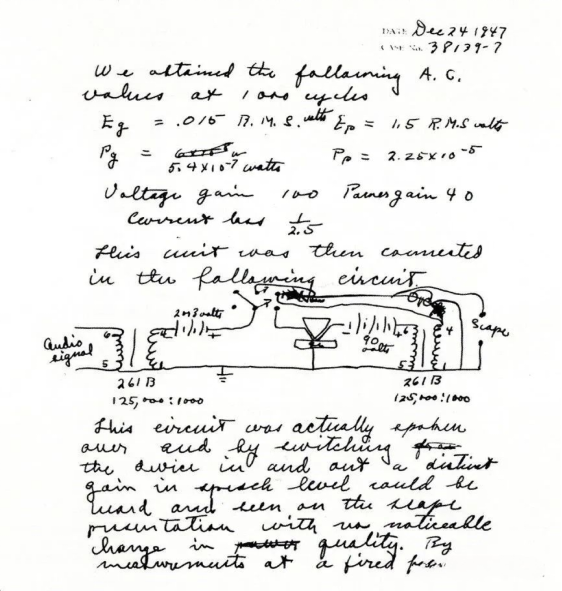
Brattain Records shown on December 23,1947
Brattain With a microphone and headphones, recording in his notebook, " This circuit has actually been discussed and...... Can be heard and seen in the oscilloscope presentation."Sadly, no one remembers what was said, just that it worked. Shockley called it a "wonderful Christmas present".
Within days of Christmas, patent agents at Bell Labs began recording their work and preparing for a public announcement. Since Shockley's self-drive and self-promotion campaign made him the most prominent face for Bell Labs, the order issued demands not to photograph Bardeen and Brattain without his presence. Promotional photographs at the time showed him on the front and centre of the site.
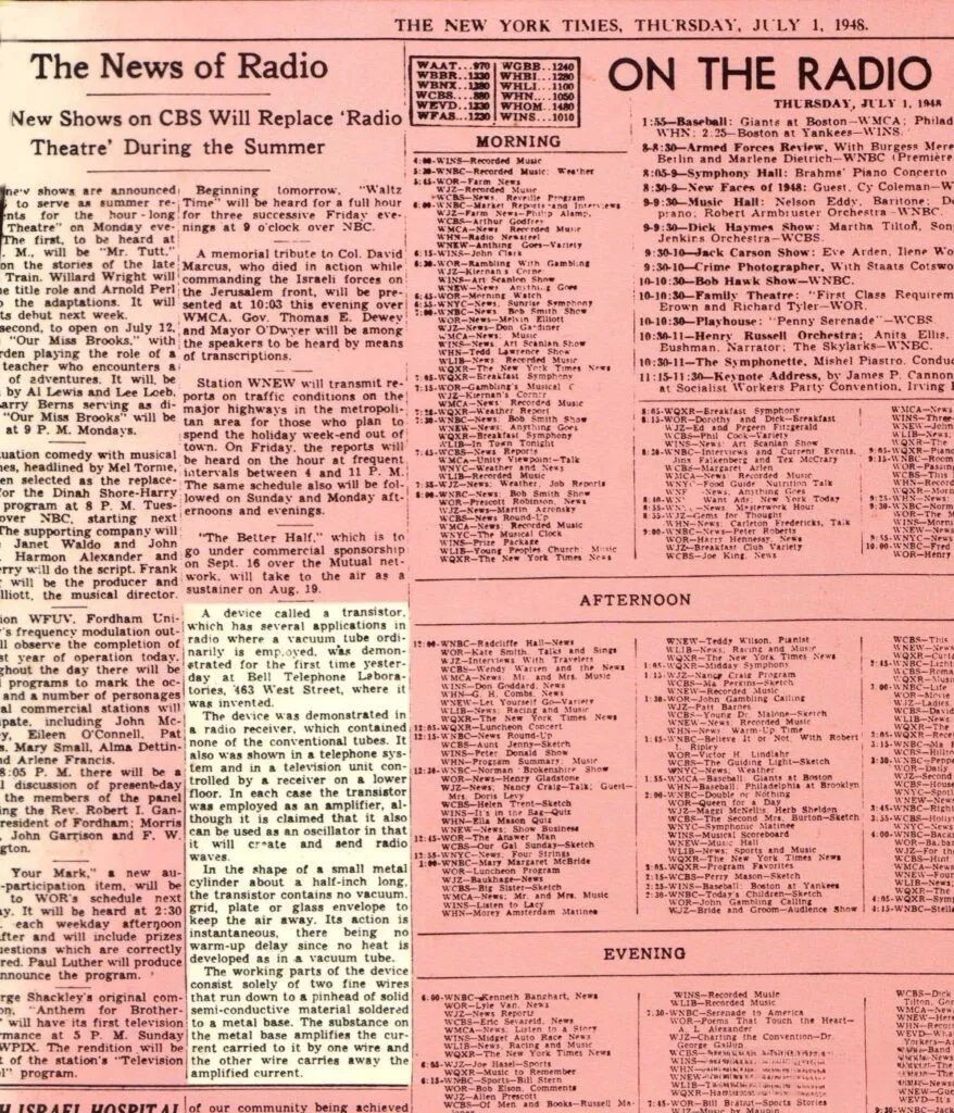
At a press conference in New York on June 30,1948, a spokesman claimed that the transistor "may have far-reaching implications in electronic and electrical communications."The New York Times, unmoved, downgraded the story to the "Radio News" page —— below the soap opera sponsor announcement.

The Brattain colleague John Pierce is credited as the one who came up with the name. He also realized that it worked on the principle of transelectric resistance, and that Pierce had derived transistors from related electronic components called resistors.
AT & T's equipment division, Western Electric, began manufacturing point-contact transistors in 1951, and by mid-1952 produced more than 6,000 devices per month, primarily for telephone switching systems and hearing aids.
According to Brattain, Shockley is pushing for some of his ideas into their patent applications, " Shortly after the presentation, Bardeen and I called us separately and told us that sometimes the people who did the job didn't get me tell him,' Oh hell, Shockley, that's enough glory for everyone."But he left alone, working from home, and in some ways was no longer a part of the research team.”
Yet based on his theoretical contributions to understanding semiconductor physics and his invention of the junction transistor, Shockley, along with Bardein and Bratton, accepted the 1956 Nobel Prize in Physics for "semiconductor research and the discovery of the transistor effect".
With jealousy not more obviously involved in the invention of the transistors and the need to maintain his position relative to his subordinate, Shockley began a month of intensive theoretical activity. He determined that the point-contact transistor operation is not a hypothetical near-surface field effect, but is due to a completely different structure in the crystal body called the PN junction.
As a result of this work, Shockley conceived on January 23,1948 of a very different element, called junction transistors, that proved more reliable and easier to mass produce than point-contact devices. Before bell laboratories announced progress on July 4,1951, manufacturing working transistors remained a daunting challenge. His version became the main active electronic building block for the coming decades by enabling a new generation of powerful computers.
It is worth mentioning that, based on his theoretical contributions to the understanding of semiconductor physics and his invention of the junction transistor, Shockley accepted the 1956 Nobel Prize in physics for "the semiconductor research and the discovery of the transistor effect".
While in the next development, many different fabrication methods were developed for faster, cheaper and more reliable transistors. An important advance in 1954 was the silicon transistor, first developed by Morris Tanenbaum at Bell Labs, and shortly after by a team led by chemist Willis Adcock at upstart Texas Instruments. By the end of the 1950s, silicon had become the industry * material, and TI became a major semiconductor supplier.
Then, Legend Announcement Fairchild launched a double-diffusion silicon countertop transistor in 1958. It's revolutionary flat process by Swiss physicist Jean Hoerni solves the reliability issues that threaten the company's future. Hoerni Planar technology not only transforms transistor manufacturing from semi-manual operation to mass automated production. It has also promoted the development of modern integrated circuits (IC).
The Coming of the MOSFET
After several years of development, the idea of Lilienfeld and Heil and Shockley's failed early experiments finally bore fruit in 1959. At that time, the Korean electrical engineer Dawon Kahng was an Egyptian engineer Martin M.(John) Atalla worked on the semiconductor surface at the Bell lab and established * successful effector transistors (FET: field-effect transistor) consisting of metal (M gate), oxide (O insulation), and silicon (S semiconductor) layers. It was also later known as MOSFET (usually MOS), making smaller, cheaper, and less power transistors possible.
Fairchild and RCA introduced commercial MOS transistors in 1964. But in the decade of solving early manufacturing problems, a single transistor in a computer system has largely been replaced by IC. In the long run, MOS transistors prove to be the most practical way to build high-density ICs (such as microprocessors and memory). Nearly 100% of the billions of transistors made every day are MOS devices.
As with most technological developments, the invention of modern transistors follows the Bacon model, which gradually emerged from the "growing knowledge base" built by a truly international community of engineers and scientists, rather than from the individual efforts of a heroic "inventor".”


 English


